
Method for removing silicon oxide film and processing apparatus

a technology of silicon oxide film and processing apparatus, which is applied in the direction of electrical apparatus, decorative surface effects, decorative arts, etc., can solve the problems of gate oxide film deterioration, gate oxide film thickness control is difficult, gate oxide film forming is not only difficult, etc., and achieves the effect of efficient removal of silicon dioxide film

Inactive Publication Date: 2009-11-03
TOKYO ELECTRON LTD
View PDF17 Cites 15 Cited by
  • Summary
  • Abstract
  • Description
  • Claims
  • Application Information

AI Technical Summary

Benefits of technology

The present invention provides a method and system for efficiently removing silicon dioxide films, such as natural oxide films or chemical oxide films, at high degrees of etch selectivity. The method involves using a mixed gas containing HF gas and NH3 gas in a processing vessel that can be evacuated. The processing temperature and pressure are set at high levels, and the silicon dioxide film is removed by etching with a high degree of selectivity to other films, such as silicon nitride or thermal oxide film. The flow rate ratio of HF gas to NH3 gas is important, and the processing pressure is set between 1011 Pa and (200 torr). The processing system includes a processing vessel, workpiece holding means, heating means, evacuating system, HF gas supply system, NH3 gas supply system, oxidizing gas supply system, and silicon film forming gas supply system.

Problems solved by technology

The natural oxide film deteriorates electrical properties.
The control of the thickness of such a gate oxide film is difficult.
Such a problem resides not only in forming the gate oxide film, but also in forming various kinds of thin film.
It takes much time to change the temperature of a processing vessel, namely, a vertical furnace, having a large heat capacity in a wide temperature range, which reduces throughput greatly.

Method used


Image

  • Method for removing silicon oxide film and processing apparatus
  • Method for removing silicon oxide film and processing apparatus
  • Method for removing silicon oxide film and processing apparatus

Examples


first embodiment

[0045]A silicon dioxide film removing method in a first embodiment according to the present invention and processing systems for carrying out the same will be described with reference to the accompanying drawings.

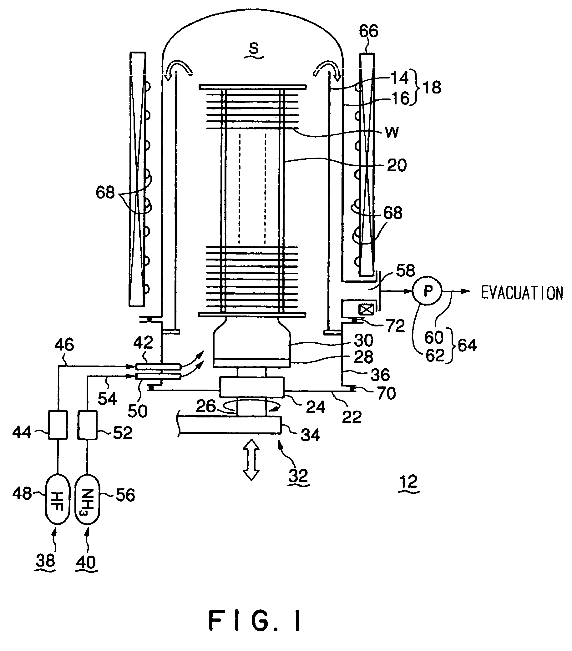
[0046]FIG. 1 shows a processing system 12 for carrying out a silicon dioxide film removing method in a preferred embodiment according to the present invention. The processing system 12 includes a double-wall, vertical processing vessel 18 of a predetermined length. The processing vessel 18 includes an inner tube 14 of quartz and an outer tube 16 of quartz. The inner tube 14 defines a processing space S. A wafer boat 20 of quartz, namely, a workpiece holding means, is placed in the processing space S. Semiconductor wafers W, namely, workpieces, are held in layers on the wafer boat 20 at predetermined vertical pitches. The pitches may be equal or may be different according to the positions of the wafers W.

[0047]A cap 22 closes and opens the lower end of the processing vessel ...

second embodiment

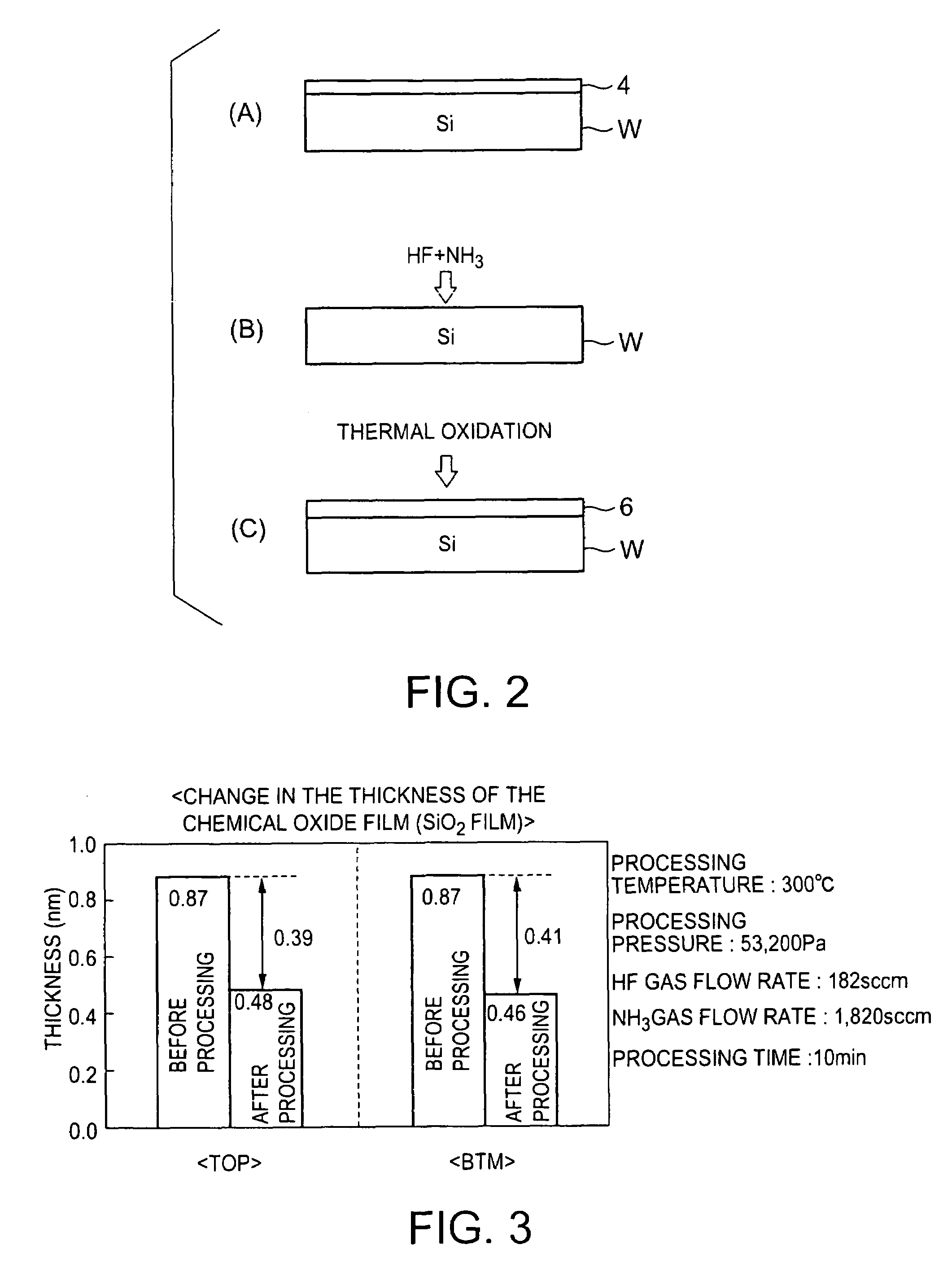
[0058]Then, a thermal oxide film 6 for forming, for example, a gate oxide film is formed on the wafer W as shown in FIG. 2(C) by another processing system. A silicon dioxide film removing method in a second embodiment, which will be described later, carries out both a film removing process for removing the chemical oxide film 4 and a film forming process for forming the thermal oxide film 6 by a single processing system.

[0059]A film removing method of removing the chemical oxide film 4 by the processing system 12 will be more specifically described.

[0060]As shown in FIG. 2(A), a plurality of semiconductor wafers W each having a surface coated with a chemical oxide film 4 are arranged in layers at predetermined pitches on the wafer boat 20. The boat elevator 32 raises the wafer boat 20 upward to load the wafer boat 20 through the lower end of the processing vessel 18 into the processing vessel 18. Then, the processing vessel 18 is sealed. The interior of the processing vessel 18 is h...


PUM

PropertyMeasurementUnit
pressureaaaaaaaaaa
pressureaaaaaaaaaa
thicknessaaaaaaaaaa

Abstract

A silicon dioxide film removing method is capable of removing a silicon dioxide film, such as a natural oxide film or a chemical oxide film, at a temperature considerably higher than a room temperature. The silicon dioxide film removing method of removing a silicon dioxide film formed on a workpiece in a processing vessel 18 that can be evacuated uses a mixed gas containing HF gas and NH3 gas for removing the silicon dioxide film. The silicon dioxide film can be efficiently removed from the surface of the workpiece by using the mixed gas containing HF gas and NH3 gas.

Description

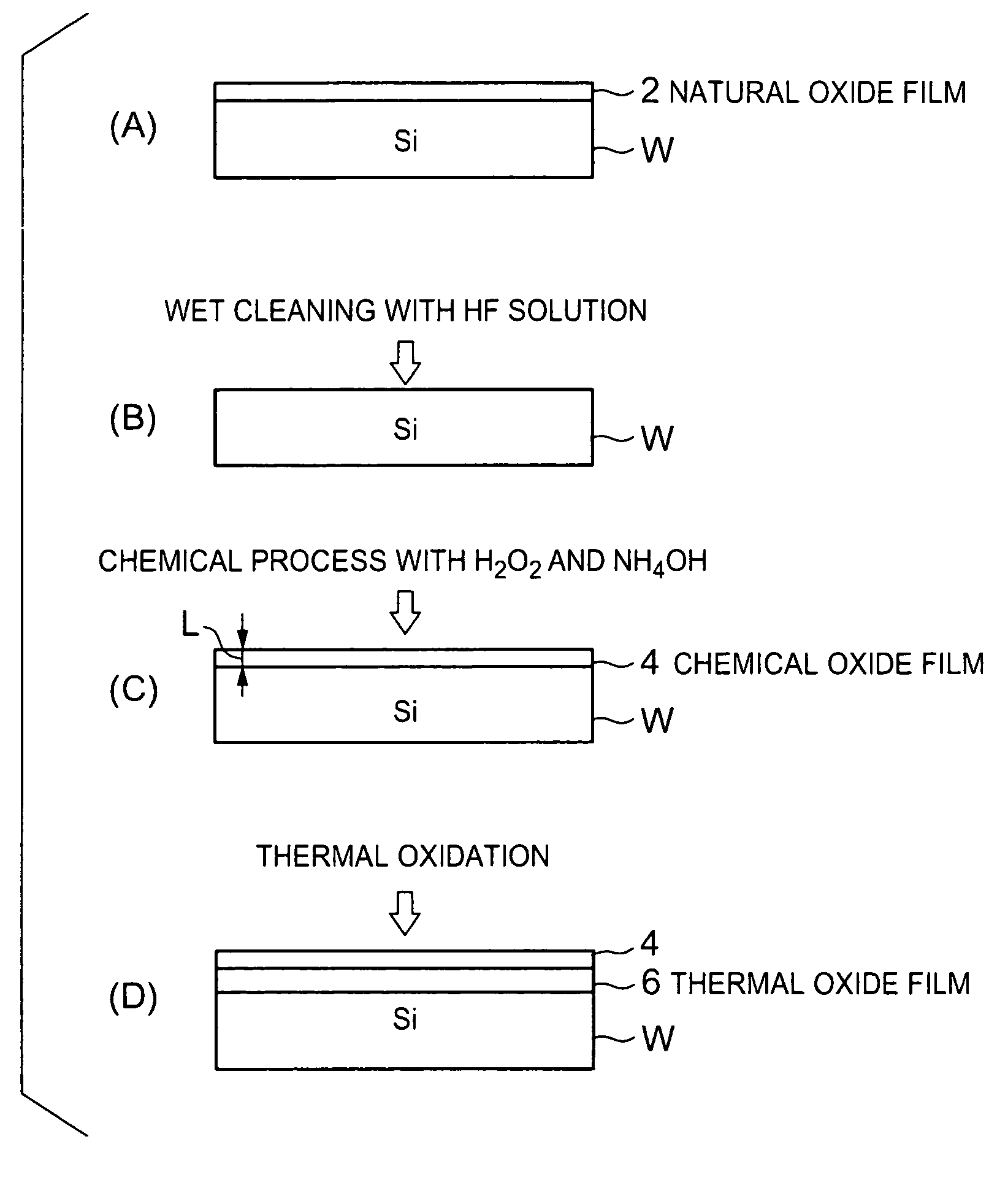
TECHNICAL FIELD[0001]The present invention relates to a method of removing a silicon dioxide film formed on a surface of a workpiece, such as a semiconductor wafer, and a processing system.BACKGROUND ART[0002]Generally, a semiconductor wafer, such as a silicon substrate, is subjected to various processes including a film forming process, an etching process, an oxidizing process, a diffusion process and modification process to fabricate a semiconductor integrated circuit on the semiconductor wafer. When the semiconductor wafer is carried from one processing vessel for the preceding process to another processing vessel for the succeeding process, the semiconductor wafer is exposed to a clean atmosphere. Oxygen and moisture contained in the atmosphere react with active silicon atoms exposed on the surface of the wafer and form a natural oxide film of SiO2. The natural oxide film deteriorates electrical properties. Therefore, the natural oxide film is removed by a wet cleaning process u...

Claims


Application Information

Patent Timeline
Patent Type & Authority Patents(United States)
IPC IPC(8): H01L21/302H01L21/3065H01L21/311
CPCH01L21/31116H01L21/302H01L21/3065
Inventor HASEBE, KAZUHIDEOKADA, MITSUHIROCHIBA, TAKASHIOGAWA, JUN
Owner TOKYO ELECTRON LTD
Learn More