Hole pattern design method and photomask

a pattern design and pattern technology, applied in the field of hole pattern design methods and photomasks, can solve the problems of affecting affecting the design of the hole pattern, so as to reduce the design man-hours, improve the overall optical condition of the pattern drawing, and improve the overall optical condition. effect of the overall optical condition

Active Publication Date: 2009-05-26
RENESAS ELECTRONICS CORP
View PDF14 Cites 4 Cited by
  • Summary
  • Abstract
  • Description
  • Claims
  • Application Information

AI Technical Summary

Benefits of technology

[0014]The present invention aims at solving the problems of the conventional technology described above, and its object is to improve the flexibility of hole pattern arrangement and provide a method of designing hole patterns where the quality of a hole pattern arrangement is easily evaluated, and a photomask made by this method.
[0028]Furthermore, since it becomes easier to evaluate the quality of each pattern arrangement of hole patterns and auxiliary patterns, the design man-hours are reduced.

Problems solved by technology

As explained above, even if techniques such as adjusting the size of auxiliary patterns or adjusting the distance between the auxiliary patterns and hole patterns are employed, problems such as a transfer of the auxiliary patterns and distortion of hole pattern shape occur.
Furthermore, when devising a realistic application of auxiliary patterns to hole patterns that are arranged arbitrarily, the work is expected to be extremely complicated and troublesome because the auxiliary pattern size and a layout including distances between the patterns have to be optimized for each pattern.
As explained, when arranging hole patterns and auxiliary patterns, it is difficult not only to arrange them, but also to secure a broad enough focus margin.
The problems described above stem from the fact that the focus margin of fine hole patterns depends heavily on the density of its layout.
Also, a dense layout where the density of hole patterns is high and a sparse layout where the density is low require remarkably different optimal exposure conditions (optical conditions, etc.) and it is essentially impossible to expose the both layouts under the same conditions and have patterns formed on a photoresist layer.

Method used


Image

  • Hole pattern design method and photomask
  • Hole pattern design method and photomask
  • Hole pattern design method and photomask

Examples


embodiment 1

[0038]A method of designing hole patterns according to the present invention will be described below. In the present embodiment, a minimum pitch allowed by a design rule for designing patterns of a photomask used during an exposure process in semiconductor integrated circuit manufacturing is the densest pitch of hole patterns.

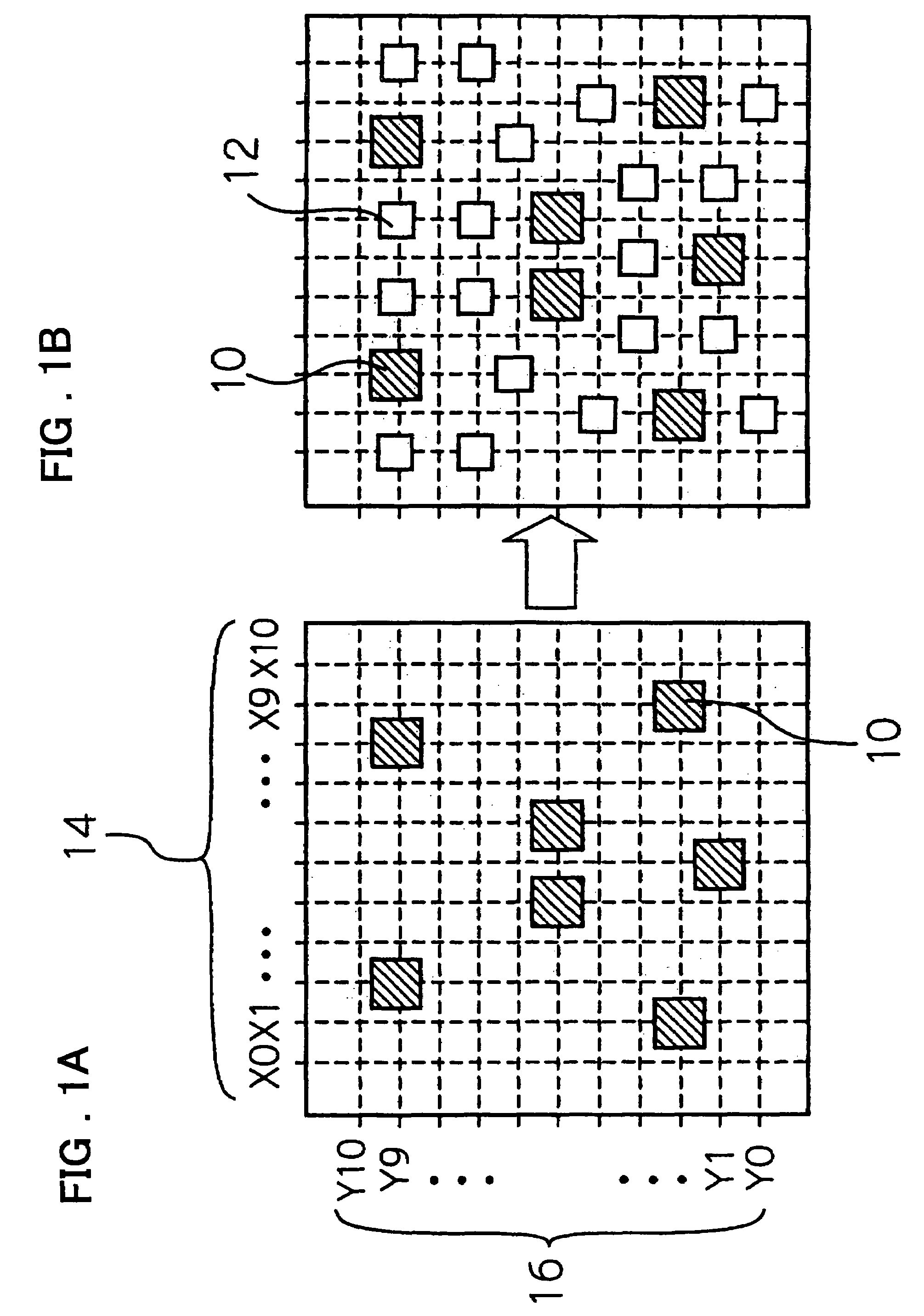
[0039]FIG. 1 shows pattern drawings showing a method of designing hole patterns on a photomask.

[0040]In FIG. 1A, the lateral direction is called X direction and the vertical direction Y direction. As shown in FIG. 1A, a grid with uniformly spaced multiple lines in X and Y directions (coordinates) is provided on the pattern drawing. The space of grid is smaller than the densest pitch of hole patterns 10. In the present embodiment, the space of the grid is half of the densest pitch of the hole pattern 10. Hereinafter, the space of grid is called “grid size”, and size of “grid size” multiplied by n (n is an integer) is indicated as “n grid sizes”. Furthermore, thi...

embodiment 2

[0048]In the present embodiment, the degree of isolating property (discreteness) from other surrounding patterns is calculated for each pattern, and an optimal pattern arrangement is realized utilizing the degree of isolating property. In the present embodiment, as a value indicating the degree of isolating property, “discreteness rate” as defined below is used.

[0049]On a pattern drawing for a photomask, a resize process, where each pattern is enlarged by a prescribed multiplier centering the gravity center, is carried out, and similar patterns, which are patterns resulted from the resize process on each pattern, are virtually created. Hereinafter, an object pattern whose discreteness rate is being calculated is called “reference pattern”, and patterns surrounding the reference pattern are called “peripheral patterns”. Furthermore, a similar pattern of the reference pattern is called “reference similar pattern”, and a similar pattern of peripheral pattern is called “peripheral simil...

embodiment 3

[0071]In the present embodiment, a optimum value of hole density, which is the area density of hole patterns within a prescribed area, is calculated and applied to a hole pattern design method.

[0072]The hole density according to the present invention is explained below.

[0073]FIG. 6 shows pattern drawings for explaining hole density. FIG. 6A shows an example where a maximum number of hole patterns are provided within a unit graphic. FIG. 6B shows a figure showing a pattern arrangement example for calculating hole density.

[0074]As shown in FIG. 6A, the unit graphic 30 is a square with a side three times as long as the densest pitch of hole patterns 10, therefore, the maximum number of the hole patterns 10 that can be provided within the unit graphic 30 is 9. In the present embodiment, in order to secure a focus margin (>0.2 μm), the number of the hole patterns 10 provided within the unit graphic 30 must be not less than 5.4 according to the graph, i.e. 6 or more in terms of the number...


PUM

PropertyMeasurementUnit
processing sizeaaaaaaaaaa
transmittanceaaaaaaaaaa

Abstract

A method of designing hole patterns for arranging hole patterns on a pattern drawing of a photomask used during an exposure process in semiconductor integrated circuit manufacturing, wherein a grid is provided on the pattern drawing with a space smaller than a minimum pitch allowed by the design rule of the semiconductor integrated circuit, and the hole patterns are provided at lattice points, which are the intersections of the grid. Flexibility of hole pattern arrangement is improved and the quality of hole pattern arrangement can be easily evaluated.

Description

FIELD OF THE INVENTION[0001]This invention relates to a photomask used for forming hole patterns such as contact holes and via holes during an exposure process in semiconductor integrated circuit manufacturing process and to a hole pattern design method for deciding the arrangement of the hole patterns on the photomask.BACKGROUND OF THE INVENTION[0002]A conventional method for arranging hole patterns is described below:[0003]FIG. 8 shows pattern drawings showing examples of hole pattern arrangement formed on a photomask.[0004]As shown in FIG. 8A, since a focus margin is not broad enough in the layout where hole patterns 10 are arranged arbitrarily, an arrangement of auxiliary patterns, which are not transferred onto a photoresist layer during an exposure process, is necessary. (Refer to Patent Document 1 for example.)[0005]As shown in FIG. 8B, in the case where auxiliary patterns 12 are arranged as densely as possible, problems where the auxiliary patterns are transferred onto a pho...

Claims


Application Information

Patent Timeline
Patent Type & Authority Patents(United States)
IPC IPC(8): G03F1/00G03F1/14G06F17/50G03C5/00G03F1/36G03F1/68G03F1/70G03F7/20G03F9/00H01L21/027H01L21/3205H01L21/768H01L23/52H01L23/522
CPCG03F1/144G03F1/30G03F7/70433G03F7/70441G03F1/36
Inventor FUJIMOTO, MASASHIMATSUURA, SEIJI
Owner RENESAS ELECTRONICS CORP
Why Eureka
Try Eureka