
Phase change random access memory and related methods of operation

a random access memory and phase change technology, applied in static storage, digital storage, instruments, etc., can solve the problems of not being able to simultaneously access 16 phase change memory cells, conventional pram devices are generally not equipped to provide currents of such high magnitudes, and achieve the effect of improving the efficiency and reliability of the devi

Active Publication Date: 2009-05-19
SAMSUNG ELECTRONICS CO LTD
View PDF11 Cites 21 Cited by
  • Summary
  • Abstract
  • Description
  • Claims
  • Application Information

AI Technical Summary

Benefits of technology

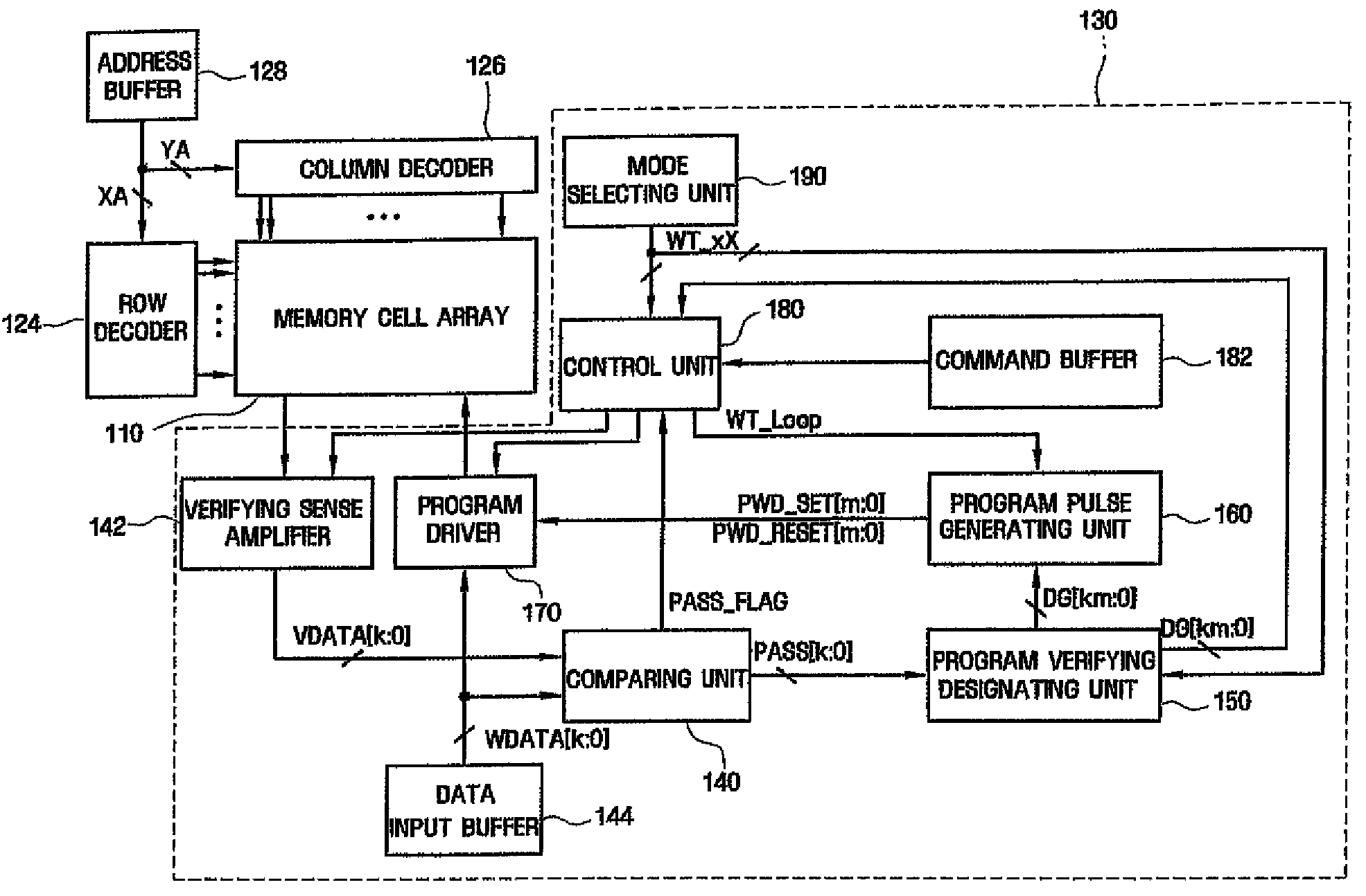
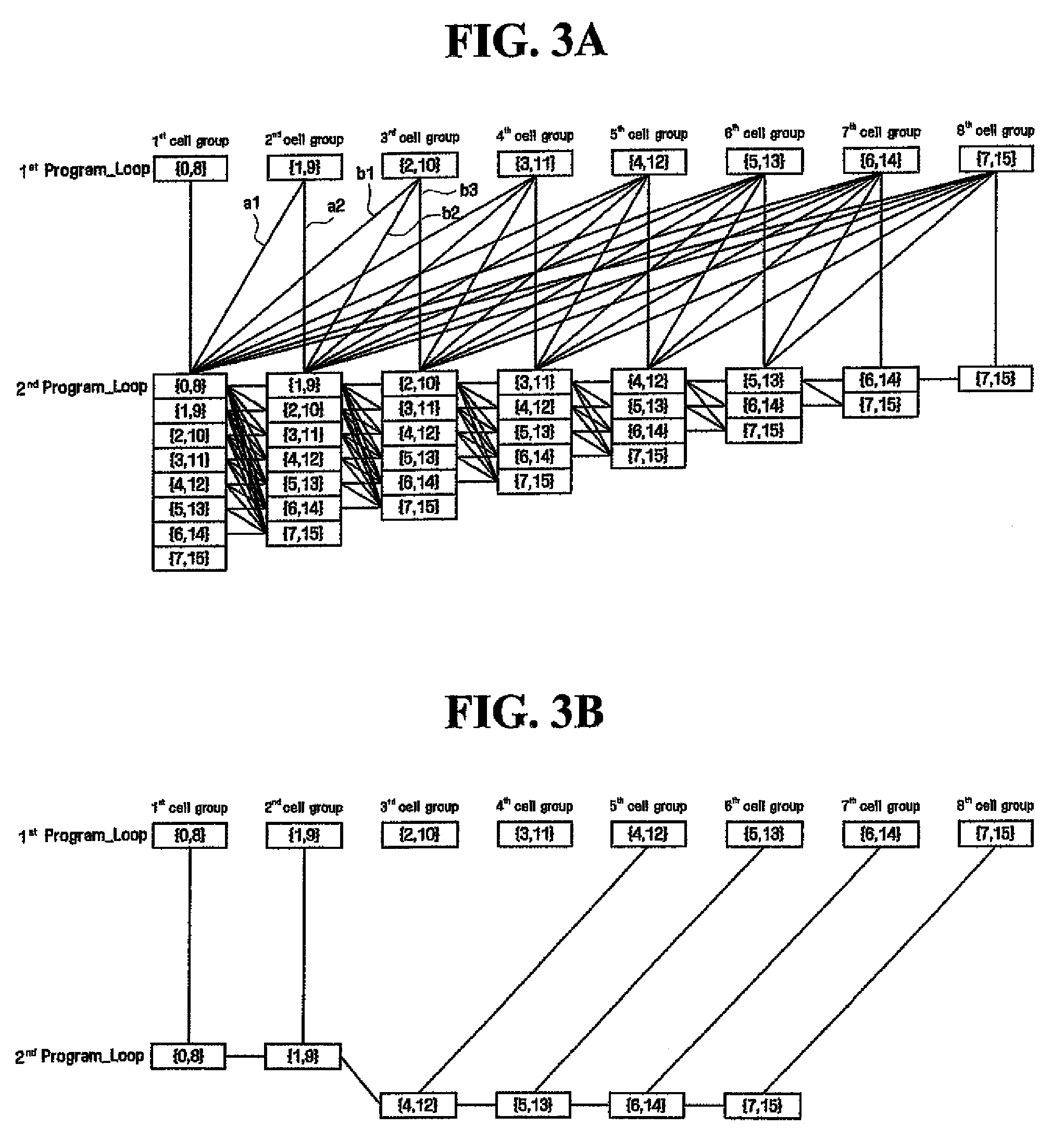
The invention provides methods and devices for improving the efficiency and reliability of phase change random access memory (PRAM) devices. The methods involve comparing verification data with program data to identify failed memory cells and then programming the failed cells with a subset of the program data using divisional program operations. The devices include a programming circuit that reads verification data from selected memory cells, performs sequential checking operations on cell groups until a failed group is detected, and performs a divisional program operation on the detected failed group. The methods and devices can improve the reliability and performance of PRAM devices.

Problems solved by technology

Unfortunately, conventional PRAM devices can receive several bits of input at the same time but are unable to simultaneously program the bits into corresponding memory cells.
For example, a PRAM may receive 16 inputs through a plurality of pins, but the PRAM may not be able to simultaneously access 16 phase change memory cells.
However, conventional PRAM devices are generally not equipped to provide currents with such high magnitudes.
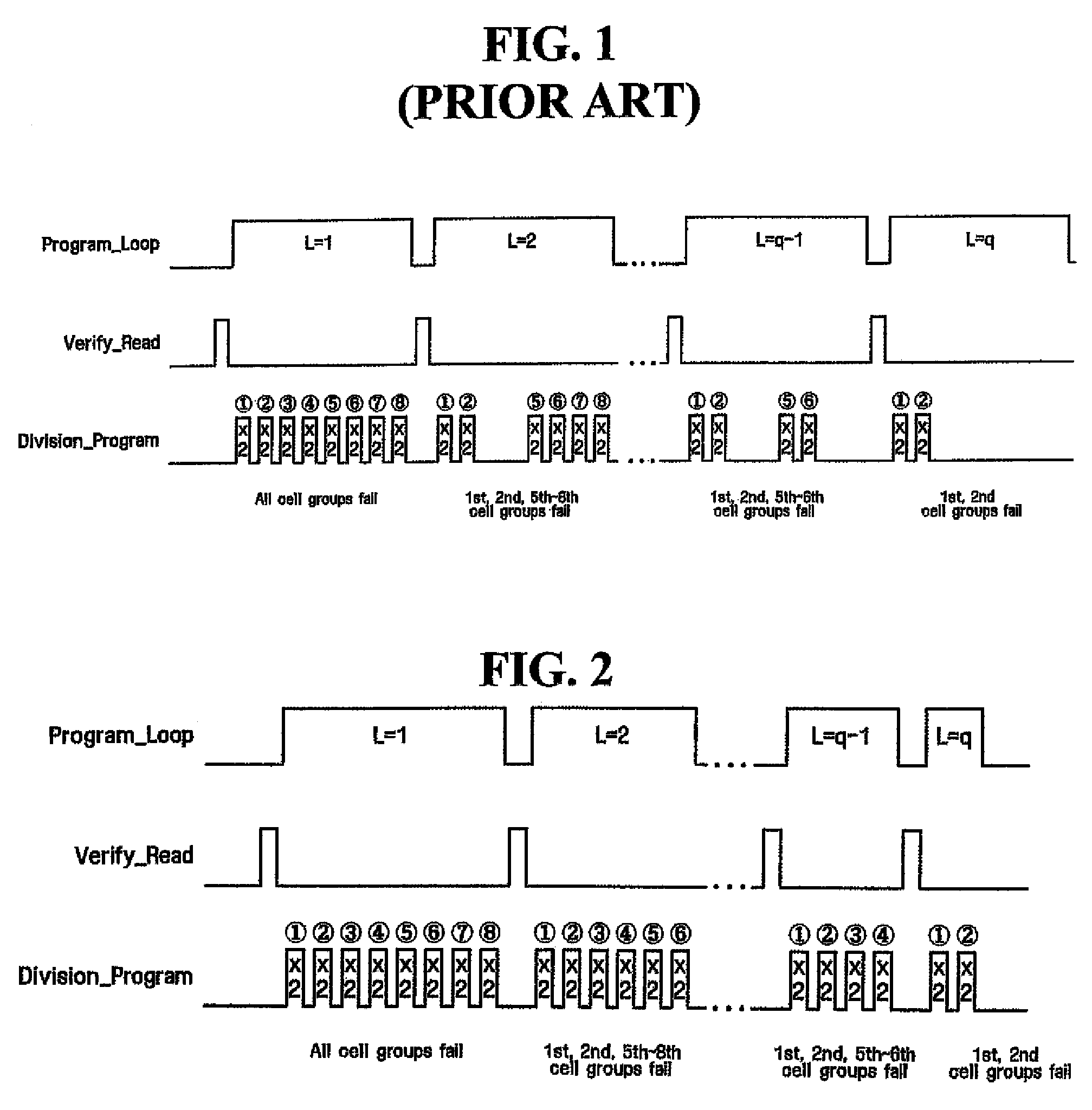
Unfortunately, conventional methods such as that illustrated in FIG. 1 may be unnecessarily slow due to time gaps where no programming is performed, such as the time gap between the second and fifth divisional program operations of the second program loop (L=2).

Method used


Image

  • Phase change random access memory and related methods of operation
  • Phase change random access memory and related methods of operation
  • Phase change random access memory and related methods of operation

Examples


Embodiment Construction

[0038]Exemplary embodiments of the invention are described below with reference to the corresponding drawings. These embodiments are presented as teaching examples. The actual scope of the invention is defined by the claims that follow.

[0039]FIG. 2 is a conceptual timing chart illustrating a method of performing a program operation in a PRAM device according to an embodiment of the invention.

[0040]Referring to FIG. 2, data is programmed to the PRAM device using a plurality of program loops. Before each program loop, a verify read operation is performed to determine whether selected memory cells have been successfully programmed. In this written description, data to be programmed in selected memory cells will be referred to as program data, and data read from the selected memory cells in a verify read operation will be referred to as verification data.

[0041]In each program loop, program data is programmed to selected cells using a plurality of divisional program operations correspond...


PUM


Abstract

In a phase change random access memory (PRAM) device, data is programmed in selected memory cells using a plurality of program loops. In each program loop, division program operations for cell groups including the selected memory cells are performed in consecutive timeslots.

Description

CROSS REFERENCE TO RELATED APPLICATIONS[0001]This application claims the priority of Korean Patent Application No. 10-2006-0084863 filed on Sep. 4, 2006, the disclosure of which is hereby incorporated by reference in its entirety.BACKGROUND OF THE INVENTION[0002]1. Field of the Invention[0003]Embodiments of the invention relate generally to phase change random access memory (PRAM) devices and related methods of operation. More particularly, embodiments of the invention relate to PRAM devices and related methods of performing program operations including divisional program operations and verify read operations.[0004]2. Description of Related Art[0005]Phase change memory devices store data using phase change materials, such as chalcogenide, which are capable of stably transitioning between amorphous and crystalline phases. The amorphous and crystalline phases (or states) exhibit different resistance values used to distinguish different logic states of memory cells in the memory device...

Claims


Application Information

Patent Timeline
Patent Type & Authority Patents(United States)
IPC IPC(8): G11C11/00
CPCG11C11/5678G11C13/0004G11C13/0064G11C13/0069G11C2013/0078G11C16/3436
Inventor LEE, KWANG-JINCHO, WOO-YEONG
Owner SAMSUNG ELECTRONICS CO LTD
Learn More