
Back-to-front via process

a back-to-front via and process technology, applied in the field of semiconductor devices, to achieve the effect of facilitating the formation of chip-to-chip electrical connections

Active Publication Date: 2009-05-19
CUFER ASSET LTD LLC
View PDF177 Cites 69 Cited by
  • Summary
  • Abstract
  • Description
  • Claims
  • Application Information

AI Technical Summary

Benefits of technology

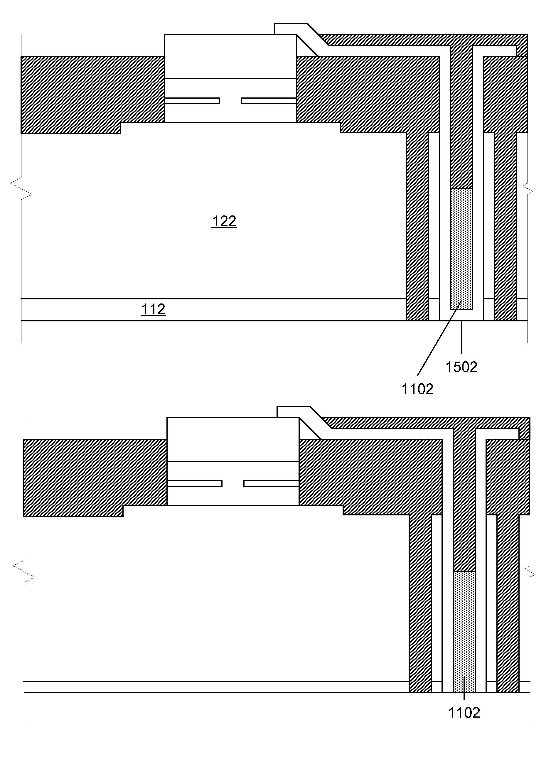
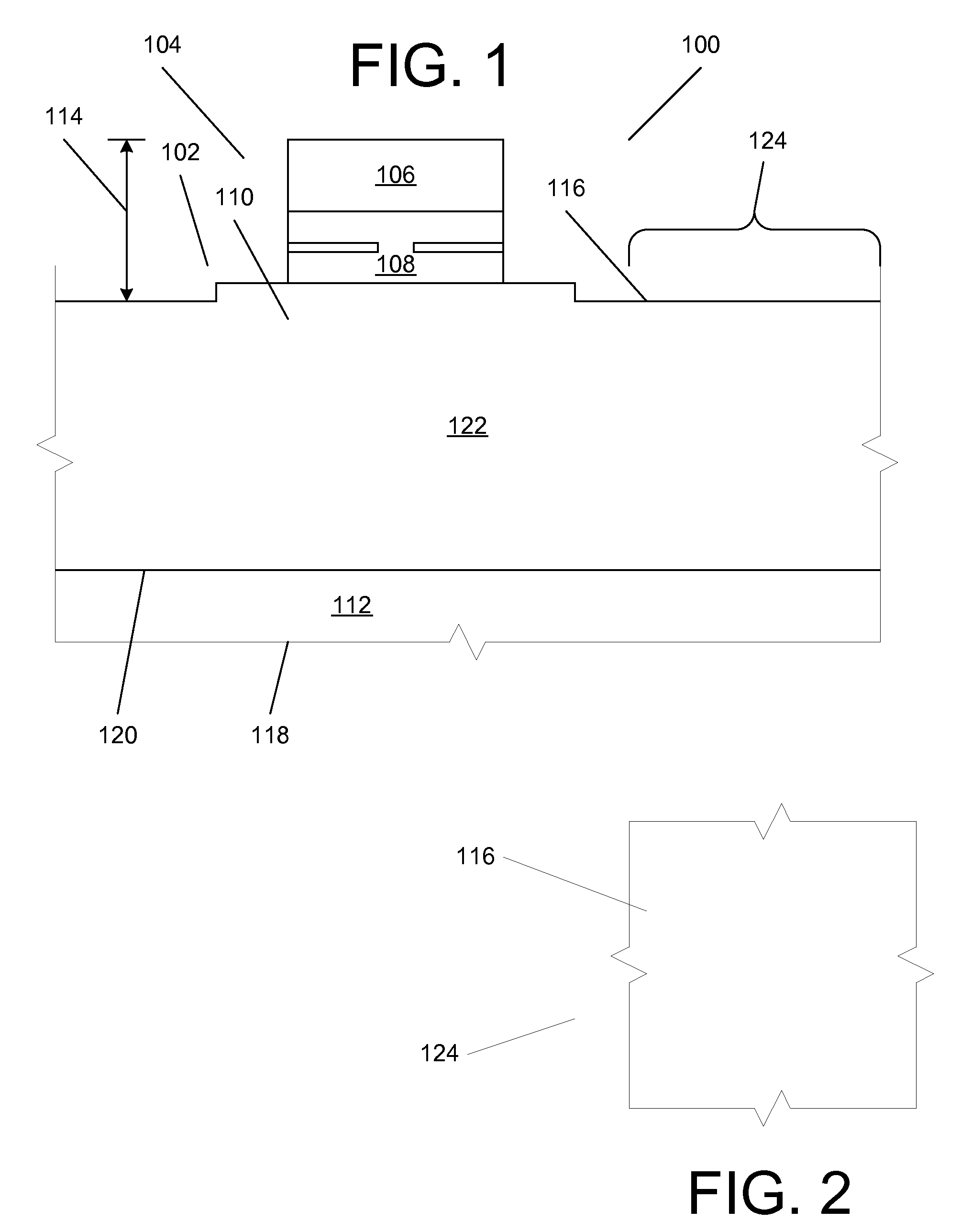
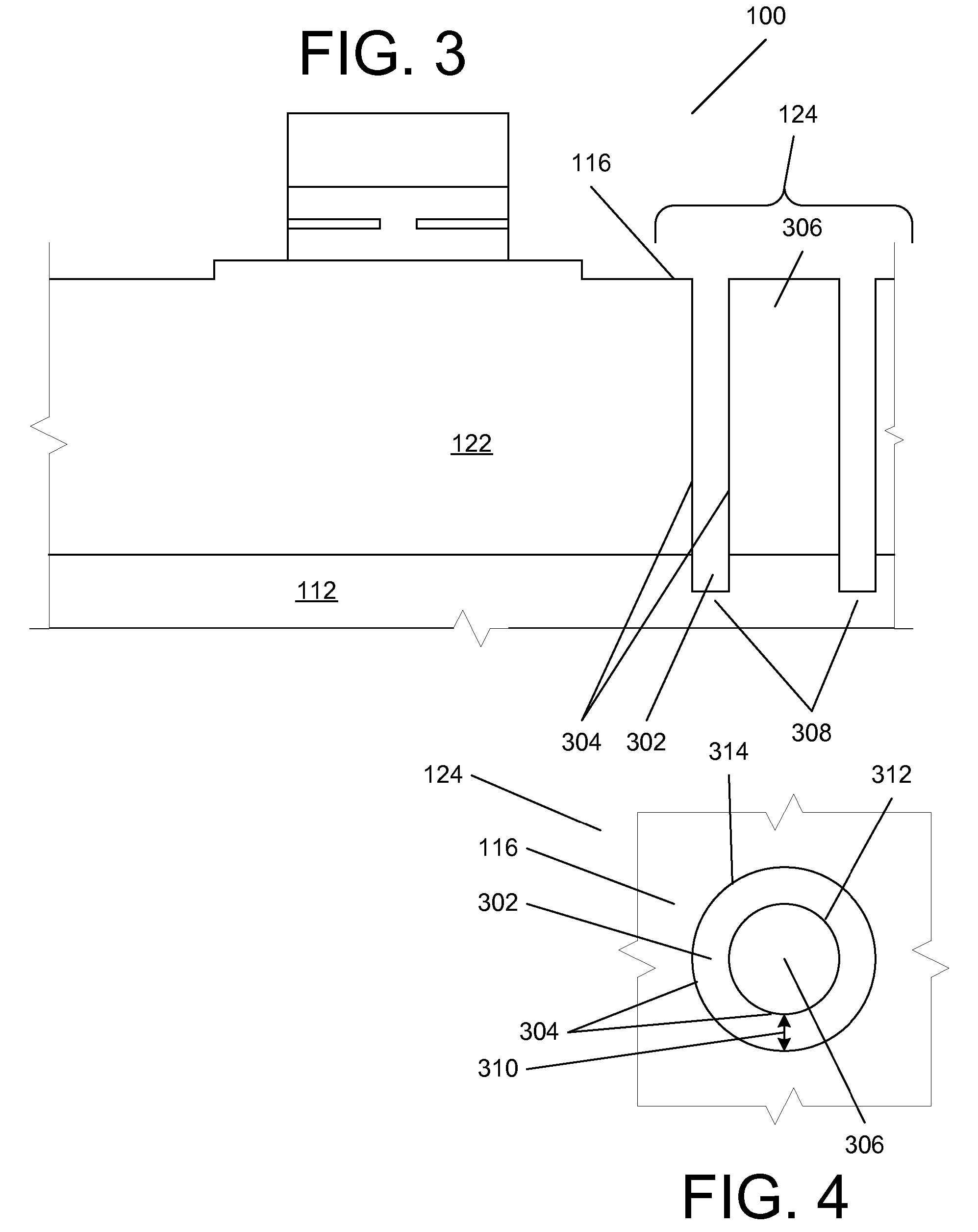
[0007]One aspect involves a method performed on a semiconductor chip having a doped semiconductor material abutting a substrate involves creating a first via through at least a portion of the substrate extending from an outer side of the substrate towards the doped semiconductor material, the first via having a wall surface and a bottom, introducing a first electrically conductive material into the first via so as to create an electrically conductive path, creating a second via, aligned with the first via, extending from an outer surface of the doped portion of the semiconductor chip to the bottom, and introducing a second electrically conductive material into the second via so as to create an electrically conductive path.
[0008]Another aspect involves forming a unit by stacking the semiconductor chip with a second semiconductor chip such that the second semiconductor chip has an electrical contact hybridized to the electrically conductive path.

Problems solved by technology

For instance, some of these advantages are mutually contradictory, in that they cannot be simultaneously present in a single embodiment.

Method used


Image

  • Back-to-front via process
  • Back-to-front via process
  • Back-to-front via process

Examples


Embodiment Construction

[0120]At the outset, it is to be understood that the term “wafer” as used herein is intended to interchangeably encompass all of the terms “chip”, “die” and “wafer” unless the specific statement is clearly and exclusively only referring to an entire wafer from which chips can be diced, for example, in references to an 8 inch or 12 inch wafer, chip or die “-to-wafer”, “wafer-to-wafer”, or “wafer scale” processing. If use of the term would, as a technical matter, make sense if replaced by the term “chip” or “die”, those terms are also intended. Moreover, a substantive reference to “wafer or chip” or “wafer or die” herein should be considered an inadvertent redundancy unless the above is satisfied.

[0121]In general, specific implementations of aspects described herein make it possible to form connections among two or more wafers containing fully-formed electronic, active optical or electro-optical devices in a simple, controllable fashion which also allows for a deep via depth, high rep...


PUM


Abstract

A method performed on a semiconductor chip having a doped semiconductor material abutting a substrate involves creating a first via through at least a portion of the substrate extending from an outer side of the substrate towards the doped semiconductor material, the first via having a wall surface and a bottom, introducing a first electrically conductive material into the first via so as to create an electrically conductive path, creating a second via, aligned with the first via, extending from an outer surface of the doped portion of the semiconductor chip to the bottom, and introducing a second electrically conductive material into the second via so as to create an electrically conductive path.

Description

[0001]This application claims priority under 35 USC 119(e)(1) of U.S. Provisional Patent Application Ser. No. 60 / 690,759, filed Jun. 14, 2005.FIELD OF THE INVENTION[0002]The present invention relates to semiconductors and, more particularly, to electrical connections for such devices.BACKGROUND[0003]Making electrical contacts that extend all the way through an electronic chip (by creating electrically conductive vias) is difficult. Doing so with precision or controlled repeatability, let alone in volume is nearly impossible unless one or more of the following is the case: a) the vias are very shallow, i.e. significantly less than 100 microns in depth, b) the via width is large, or c) the vias are separated by large distances, i.e. many times the via width. The difficulty is compounded when the vias are close enough for signal cross-talk to occur, or if the chip through which the via passes has a charge, because the conductor in the via can not be allowed act as a short, nor can it c...

Claims


Application Information

Patent Timeline
Patent Type & Authority Patents(United States)
IPC IPC(8): H01L21/44H01L21/4763H01L23/40H01L23/48H01L23/52H01L29/40
CPCH01L21/6835H01L21/76898H01L23/427H01L23/48H01L23/481H01L23/49827H01L23/5389H01L23/552H01L23/66H01L24/11H01L24/24H01L24/81H01L24/94H01L25/0652H01L25/0657H01L25/50H01L24/13H01L24/75H01L24/27H01L2221/68368H01L2223/6616H01L2223/6622H01L2224/1147H01L2224/13099H01L2224/13609H01L2224/16H01L2224/24226H01L2224/274H01L2224/75305H01L2224/81136H01L2224/81193H01L2224/81801H01L2225/06513H01L2225/06524H01L2225/06527H01L2225/06541H01L2924/01002H01L2924/01004H01L2924/01005H01L2924/01012H01L2924/01013H01L2924/01015H01L2924/01018H01L2924/01022H01L2924/01025H01L2924/01027H01L2924/01029H01L2924/0103H01L2924/01032H01L2924/01033H01L2924/01042H01L2924/01046H01L2924/01047H01L2924/01049H01L2924/01051H01L2924/01061H01L2924/01073H01L2924/01074H01L2924/01075H01L2924/01078H01L2924/01079H01L2924/01082H01L2924/04953H01L2924/09701H01L2924/10329H01L2924/14H01L2924/19041H01L2924/19043H01L2924/30105H01L2924/3011H01L2924/3025H01L2924/01006H01L2924/01023H01L2924/01024H01L2924/0105H01L2924/014H01L2924/3512H01L2924/00H01L2924/10253H01L2924/0001H01L2224/05027H01L2224/05022H01L2224/05026H01L2224/0508H01L2224/05573H01L2224/05568H01L2224/05023H01L2224/05001H01L2224/05572H01L2224/05147H01L2224/05644H01L2224/05655H01L2224/05664H01L2224/05666H01L2924/00014H01L21/28H01L21/3205H01L23/52
Inventor TREZZA, JOHN
Owner CUFER ASSET LTD LLC
Learn More