
Cell processor atomic compare and swap using dedicated synergistic processor element

a cell processor and processor element technology, applied in computing, instruments, electric digital data processing, etc., can solve the problems of ppu and spu having different reservations sizes, ppu's memory access is generally limited, application is notified of a failure,

Active Publication Date: 2009-03-24
SONY COMPUTER ENTERTAINMENT INC
View PDF7 Cites 5 Cited by
  • Summary
  • Abstract
  • Description
  • Claims
  • Application Information

AI Technical Summary

Benefits of technology

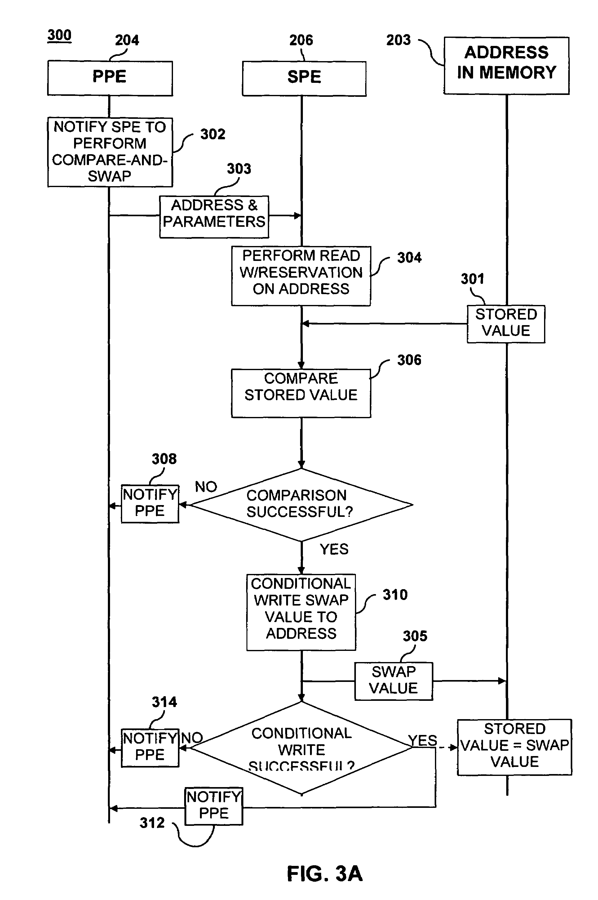
The invention is about a way to compare and change values in a computer processor system. The system has a main memory, a power processor element (PPE), and a synergistic processor element (SPE). The SPE has more memory transfer capabilities than the PPE. The PPE sends a message to the SPE to compare and change a value in memory. The SPE performs the compare and change operation quickly and informs the PPE of the success or failure of the operation. This allows the SPE to take advantage of its efficiency in performing the compare and change operation on behalf of the PPE.

Problems solved by technology

If they do not match, the application is notified of a failure.
A problem with atomic operations on cell processors is that the PPU and SPU have different reservations sizes for atomic operations.
The PPU's memory access, is generally limited by the register size of the PPU core.
It is very powerful that the SPU can work atomically on large chunks of data and it can be quite crippling that the PPU can only work atomically on 8 bytes at a time.
Such different sizes for atomic reservations can limit the features of a lock-free algorithm.
However, if larger atomics are available, one can apply lock-free algorithms to more complex operations since more than one integer may be atomically modified at a time.

Method used


Image

  • Cell processor atomic compare and swap using dedicated synergistic processor element
  • Cell processor atomic compare and swap using dedicated synergistic processor element
  • Cell processor atomic compare and swap using dedicated synergistic processor element

Examples


Embodiment Construction

[0017]Although the following detailed description contains many specific details for the purposes of illustration, anyone of ordinary skill in the art will appreciate that many variations and alterations to the following details are within the scope of the invention. Accordingly, the exemplary embodiments of the invention described below are set forth without any loss of generality to, and without imposing limitations upon, the claimed invention.

[0018]Embodiments of the present invention implement an SPU-sized Compare-and-Swap operation for the PPU in a cell processor. Such embodiments involve interoperation between SPUs and the PPU in the cell processor. Since there is a non-negligible latency overhead for the PPE to communicate with an SPE, it is desirable for the PPE to communicate with the SPE as little as possible during the compare-and-swap operation.

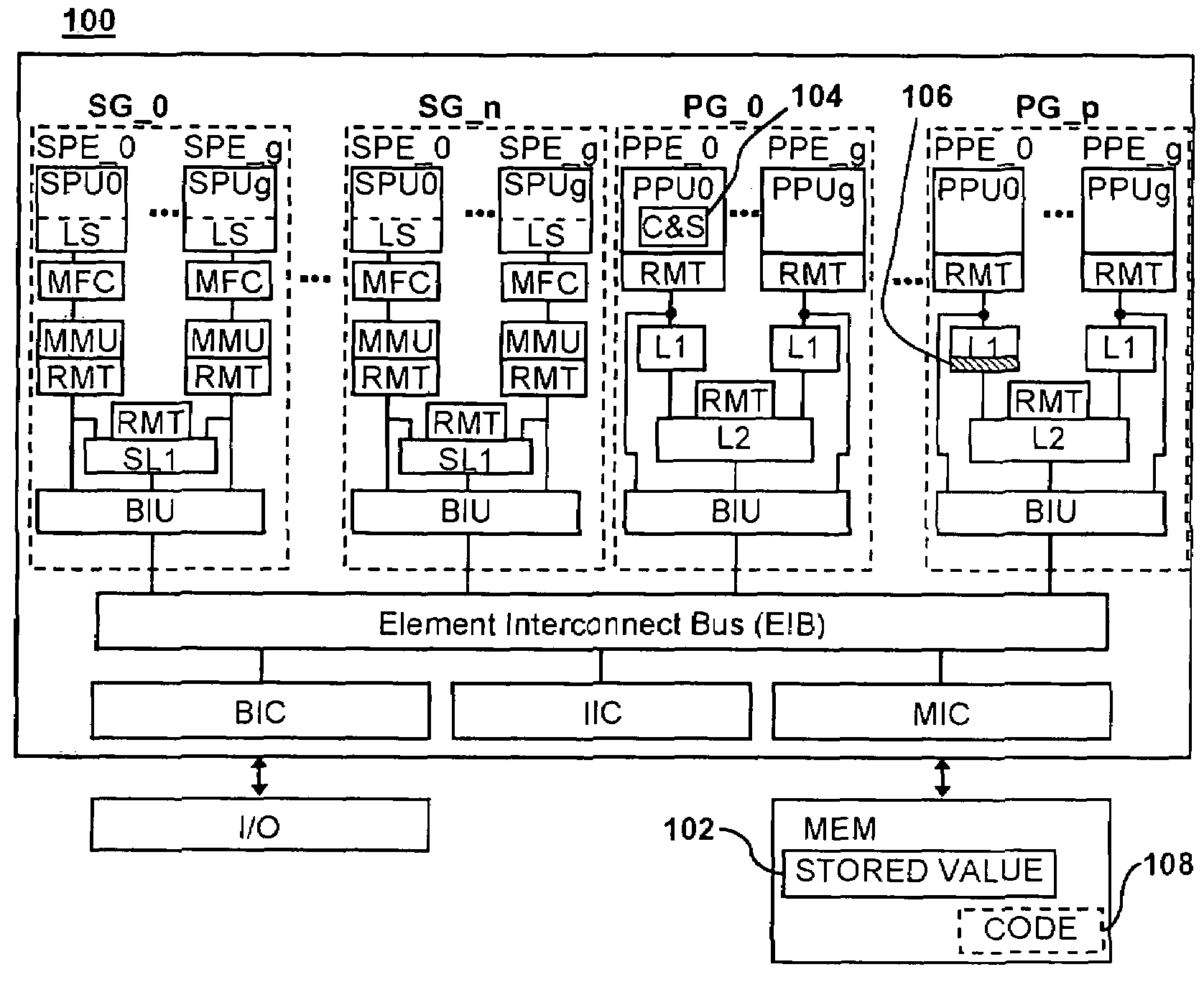
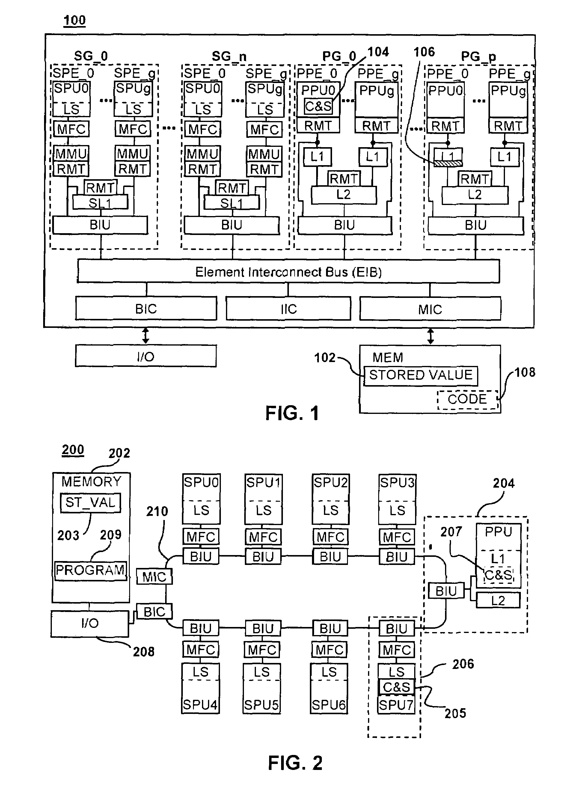
[0019]By way of example, and without limitation, FIG. 1 illustrates a type of cell processor 100 characterized by an architectur...


PUM


Abstract

An atomic compare and swap operation that can be implemented in processor system having a power processor element (PPE) and a synergistic processor element (SPE) that have different sized memory transfer capabilities. The PPE notifies an SPE to perform a compare and swap operation on an address in main memory. The address has a size less than or equal to a maximum memory transfer size for the SPE and greater than a maximum memory transfer size for the PPE. The SPE atomically performs the compare and swap operation and notifies the PPE of the success or failure of the compare and swap operation.

Description

CROSS-REFERENCE TO RELATED APPLICATION[0001]This application is related to commonly-assigned U.S. patent application 11 / 291,306 entitled “OPERATION INVOLVING PROCESSORS WITH DIFFERENT MEMORY TRANSFER OPERATION SIZES”, now U.S. Pat. No. 7,398,368 to James E. Marr John P. Bates and Tatsuya Iwamoto, which is filed the same day as the present application, the entire disclosures of which are incorporated herein by reference.FIELD OF THE INVENTION[0002]This invention relates to cell processors and more particularly to atomic operations with cell processors.BACKGROUND OF THE INVENTION[0003]Cell processors are a type of microprocessor that utilizes parallel processing. The basic configuration of a cell processor includes a “Power Processor Element” (“PPE”) (sometimes called “Processing Element”, or “PE”), and multiple “Synergistic Processing Elements” (“SPE”). The PPEs and SPEs are linked together by an internal high speed bus dubbed “Element Interconnect Bus” (“EIB”). Cell processors are d...

Claims


Application Information

Patent Timeline
Patent Type & Authority Patents(United States)
IPC IPC(8): G06F9/312
CPCG06F9/30021G06F9/3004G06F9/30087
Inventor MARR, JAMES E.BATES, JOHN P.
Owner SONY COMPUTER ENTERTAINMENT INC
Learn More