
Charging guard with paschen stacking

a charging guard and paschen technology, applied in the field of microelectro mechanical system devices, can solve the problems of severe physical damage to any surface exposed, breakdown of any surface along the surface, and limited maximum voltage that can be applied, so as to reduce exposure to uncontrolled surface potentials, avoid voltage drift, and apply high voltage

Inactive Publication Date: 2009-03-24
GLIMMERGLASS NETWORKS
View PDF6 Cites 0 Cited by
  • Summary
  • Abstract
  • Description
  • Claims
  • Application Information

AI Technical Summary

Benefits of technology

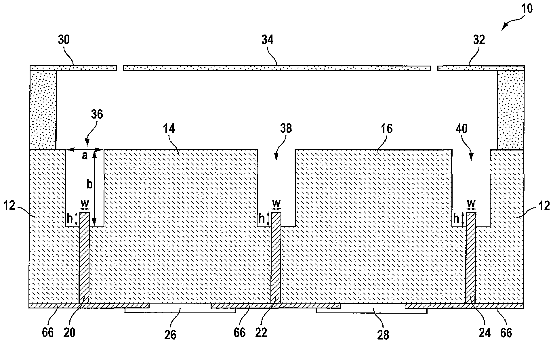
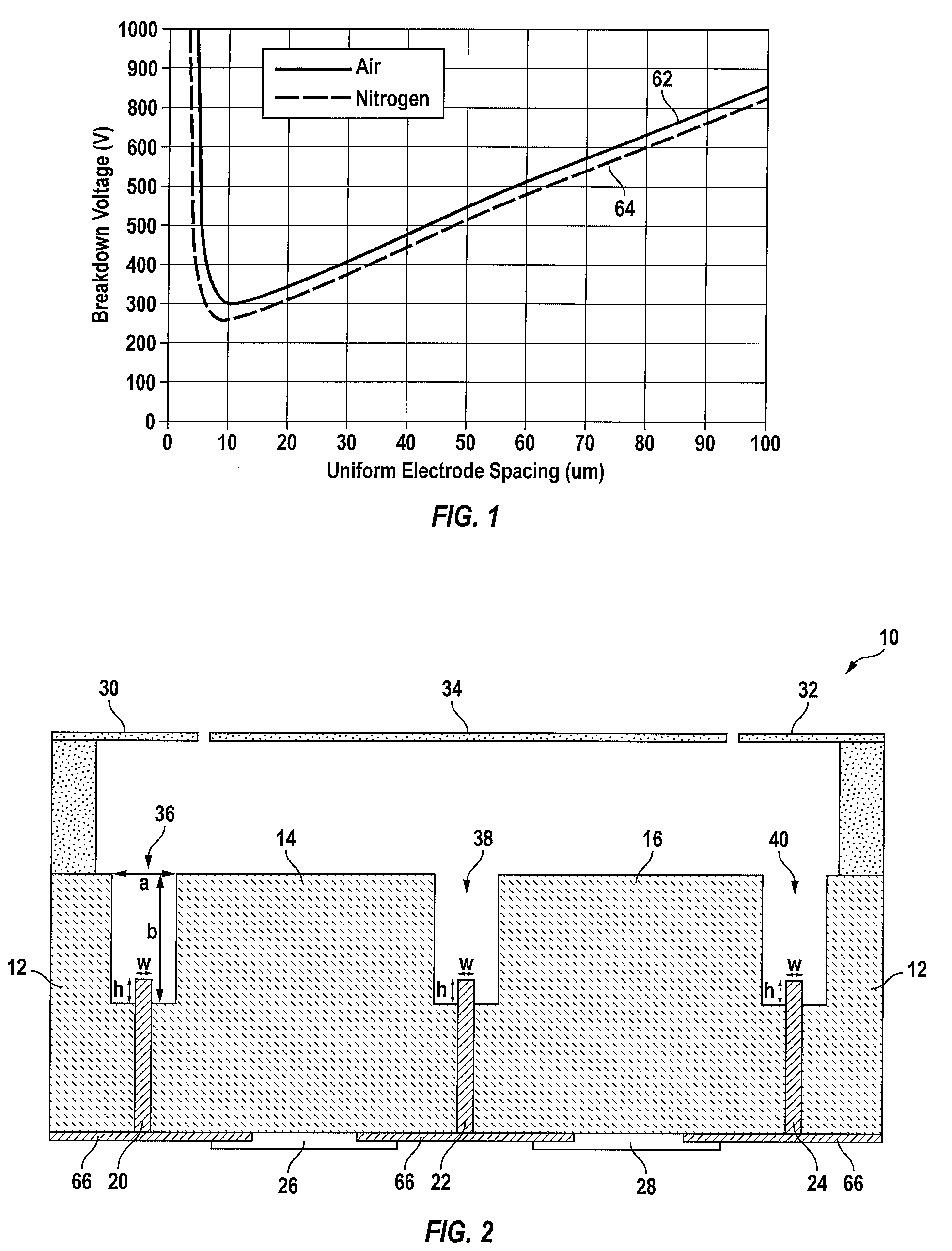
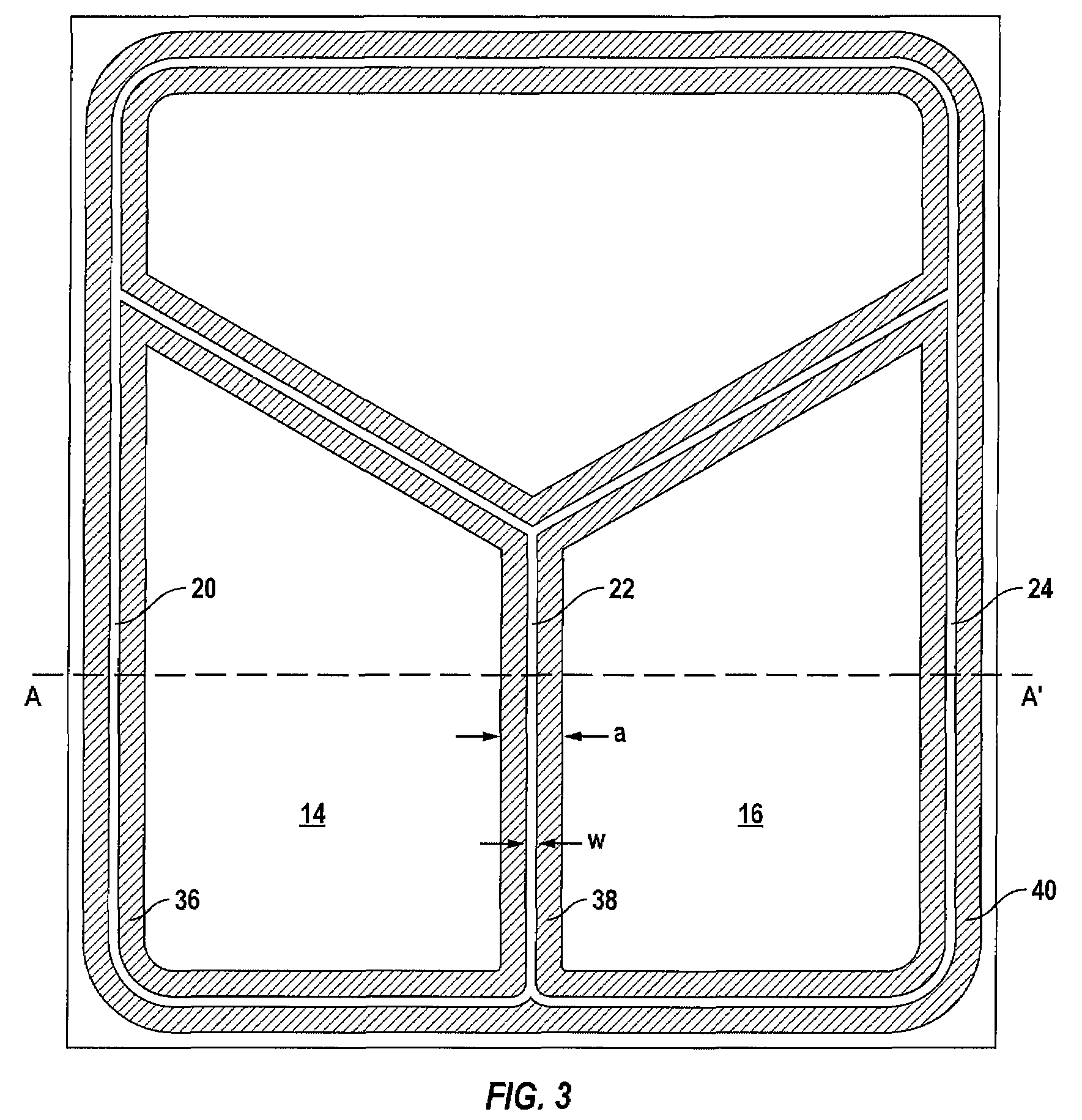
[0008]A MEMS-based mirror, is adapted to withstand relatively high applied voltages and has a substantially reduced exposure to uncontrolled surface potentials by the provision of trenches between adjacent electrodes of the MEMS-based mirror. The MEMS-based mirror, accordingly, avoids voltage drifts and has an improved mirror position stability. The trench dimensions are selected such that the voltage applied between each adjacent pair of electrodes stays within predefined limits, as determined, for example, by the Paschen curve.
[0009]In one embodiment, the electrodes (conductive elements) are formed in a silicon substrate. An insulating layer, such as silicon dioxide is used to electrically isolate the electrodes from one another and from the rest of the substrate. Each insulting layer extends partially above an associated trench. In some embodiments, the height of the extension is 2 to 4 times the width of the extensions. The insulating layer extensions that protrude from a bottom surface of their associated trenches provide a greater path length along the insulator surfaces that separate the electrodes from each other and from the rest of the substrate. A greater path length mitigates surface breakdown effects and thus, in conjunction with the trench discussed above, allows for relatively large voltages to be applied to the electrodes.
[0010]To reduce exposure to uncontrolled surface potentials, the top surface of the insulating layer is substantially recessed from the top surface of the electrodes. Any charges that accumulate on the insulator will be shielded by the conductive sidewalls of the trench thereby reducing the device susceptibility to surface potential drift on the insulators.
[0011]To further increase the range of voltages that may be applied to the MEMS-based mirror of the present invention, a multitude of trenches is disposed between the electrodes receiving these voltages. Each trench is characterized by the same depth and the same width. The trench heights may be different from the trench widths. The insulating layer electrically isolating each electrode extends upwardly from the bottom surface of each trench and it is substantially recessed from the top surface of the electrodes. The multitude of trenches electrically isolating each electrode allows one to cascade the applied voltage to an arbitrarily high value depending on the number of such trenches.

Problems solved by technology

In practice, the maximum voltage that can be applied is limited by the well understood voltage breakdown effects.
Breakdown is characterized by an uncontrolled discharge of electrical energy, which can cause severe physical damage to any surfaces exposed to the discharge.
In addition to breakdown of the ambient gas, breakdown can also occur along surfaces.
If two conductors are separated by an insulator, breakdown can occur along the surface of the insulator.
Whether breakdown occurs through the gas or on the surface, safe operation of MEMS devices using electrostatic actuation must occur below voltages that would result in breakdown.
This constraint places practical limits on the design of electrostatic MEMS devices such as the MEMS mirror mentioned above.
Another common problem encountered in electrostatic MEMS devices is control of the surface potentials between the electrodes and various insulating surface layers.
Surface potentials on dielectric surfaces are prone to drift over time due to charge migration along dielectric surfaces between the electrodes.
This can cause serious problems regarding repeatability of the mirror positioning.
The conduction characteristics of these surfaces are inherently unstable due to sensitivity to temperature, moisture and other environmental factors.
The conductivity of these surfaces is also strongly affected by impurities and process steps and materials used in the deposition and etching of the surfaces.
All of these factors combined contribute to a loss of control of the surface potentials that contribute to the forces and torques applied to the actuable elements resulting in an unreliable and uncontrollable device.

Method used


Image

  • Charging guard with paschen stacking
  • Charging guard with paschen stacking
  • Charging guard with paschen stacking

Examples


Embodiment Construction

[0018]FIG. 2 is a cross-sectional view of a MEMS-based mirror 10, in accordance with one embodiment of the present invention. As described below, MEMS-based mirror 10 is adapted to withstand relatively high applied voltages, and has a substantially reduced exposure to uncontrolled surface potentials, thereby avoiding voltage drifts and mirror position instability.

[0019]As seen from FIG. 2, electrodes 14 and 16 are electrically isolated from the rest of the substrate via insulators 20 and 24 and electrically isolated from one another via insulator 22. In the exemplary embodiment 10 of the MEMS-based mirror, the electrodes as well as supporting structures 30, 32 that support mirror 34 are formed using silicon and thus have matching thermal expansion coefficient to the electrodes and base material. In such embodiments, insulating layers 20, 22 and 24 may be formed using silicon dioxide. Metal pads 26 and 28 are used to apply voltages to electrodes 14 and 16. Although not shown, it is u...


PUM

PropertyMeasurementUnit
breakdown voltageaaaaaaaaaa
voltageaaaaaaaaaa
widthaaaaaaaaaa

Abstract

A MEMS-based mirror is provided with trenches between adjacent electrodes in order to be able to withstand relatively high applied voltages, and thus has a substantially reduced exposure to uncontrolled surface potentials. The MEMS-based mirror, thus avoids voltage drifts and has an improved mirror position stability. The trench dimensions are selected such that the voltage applied between each adjacent pair of electrodes stays within predefined limits. An insulating layer, such as silicon dioxide, electrically isolates each pair of adjacent electrodes. Each insulting layer extends partially above an associated trench and is characterized by the same height and width dimensions.

Description

BACKGROUND OF THE INVENTION[0001]The present invention relates to micro-electro mechanical system (MEMS) devices, and more particularly, to MEMS mirrors adapted to operate safely under high applied voltages.[0002]A MEMS device is typically formed, in part, using well known integrated circuit (IC) fabrication processes. One such device is a gimbaled mirror adapted to pivot in response to electrostatic actuation. The mirror's motion is used to redirect light beams. Electrostatic actuation is often achieved via capacitive action between electrodes formed on a planar surface of a substrate and the mirror positioned above the electrode. To obtain a relatively large range of angular motion, the mirror is suspended at a relatively large distance above the electrodes. Accordingly, a relatively large voltage is often necessary to cause the actuation.[0003]In practice, the maximum voltage that can be applied is limited by the well understood voltage breakdown effects. For example, if two flat...

Claims


Application Information

Patent Timeline
Patent Type & Authority Patents(United States)
IPC IPC(8): G02B26/00G02B26/08G02F1/29
CPCG02B26/0841
Inventor STAKER, BRYAN P.FERNANDEZ, ANDRESOWENS, WINDSORKINDWALL, ALEXANDER P.
Owner GLIMMERGLASS NETWORKS
Learn More