Beam tilting patch antenna using higher order resonance mode
a patch antenna and higher-order technology, applied in the field of patch antennas, can solve the problems of patch antennas not being typically disposed on the windows of vehicles, obtuse-looking devices, and bulky sdars-compliant antennas,
- Summary
- Abstract
- Description
- Claims
- Application Information
AI Technical Summary
Benefits of technology
Problems solved by technology
Method used
Image
Examples
first embodiment
[0035]Referring to FIG. 2, showing the invention, the antenna 20 includes a radiating element 30 formed of an electrically conductive material as described below. The radiating element 30 is also commonly referred to by those skilled in the art as a “patch” or a “patch element”. The radiating element 30 preferably defines a generally rectangular shape, specifically a square shape. Each side of the radiating element 30 measures about ¼ of an effective wavelength λ of the RF signal to be received by the antenna 20. RF signals transmitted by SDARS providers typically have a frequency from 2.32 GHz to 2.345 GHz. Specifically, XM Radio broadcasts at a center frequency of 2.338 GHz. Therefore, each side of the radiating element 30 measures about 24 mm. However, those skilled in the art realize alternative embodiments where the radiating element 30 defines alternative shapes and sizes based on the desired frequency and other considerations.
[0036]The antenna 20 also includes a ground plane ...
second embodiment
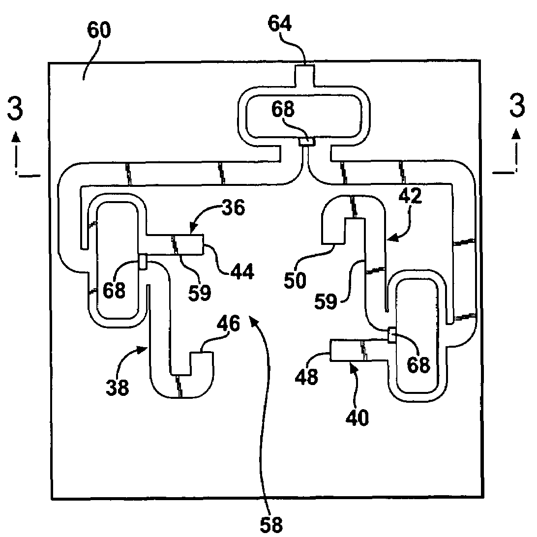
[0048]FIGS. 7 and 8 show the second embodiment where there is a direct connection between the feed lines 36, 38, 40, 42 and the radiating element 30. In this embodiment, the ground plane 32 is sandwiched between the first and second dielectric layers 60, 62. The feed line network 58 is disposed on the first dielectric layer 60 on the opposite side from the ground plane 32. A plurality of pins 64 electrically connect the feed lines to the radiating element 30. Passage holes (not numbered) are defined in the ground plane 32 to prevent an electrical connection between the feed lines 36, 38, 40, 42 and the ground plane 32.
[0049]In both the first and second embodiments, the feed line network 58 is also utilized to shift the phase of a signal applied to the feed lines 36, 38, 40, 42, thus, acting as the phase shift circuits 51 described above. This phase shifting is accomplished due to the inductive and capacitive properties of the conductive strips 59 of the feed line network 58. The ind...
third embodiment
[0052]The antenna 20 may also include at least one parasitic structure 66 for further directing and / or tilting the radiation beam. Referring now to FIG. 9, which shows the invention, the parasitic structure 66 is disposed adjacent to the radiating element 30 and separated from the radiating element 30. Said another way, the parasitic structure 66 is not in direct contact with the radiating element 30. However, the proximity of the parasitic structure 66 with the radiating element 30 affects the radiating beam. Preferably, the parasitic structure 66 is disposed substantially co-planar with the radiating element 30. It is also preferred that each of the parasitic structures 66 includes a plurality of strips 67 formed of an electrically conductive material. However, those skilled in the art realize other techniques for forming the parasitic structures 66, other than the preferred plurality of strips 67.
[0053]As stated above, the radiating element 30 defines a generally rectangular shap...
PUM
 Abstract
Description
Claims
Application Information
 - R&D
- Intellectual Property
- Life Sciences
- Materials
- Tech Scout
- Unparalleled Data Quality
- Higher Quality Content
- 60% Fewer Hallucinations
Browse by: Latest US Patents, China's latest patents, Technical Efficacy Thesaurus, Application Domain, Technology Topic, Popular Technical Reports.
© 2025 PatSnap. All rights reserved.Legal|Privacy policy|Modern Slavery Act Transparency Statement|Sitemap|About US| Contact US: help@patsnap.com


