
Method and system for providing domain wall assisted switching of magnetic elements and magnetic memories using such magnetic elements

a technology of magnetic elements and domain walls, applied in the field of magnetic random access memories, can solve the problems of high reliability issues, increase in power consumption of mrams using conventional magnetic elements b>10/b>, and unsuitability of write schemes for higher densities, and achieve the effect of low write curren

Inactive Publication Date: 2009-02-03
SAMSUNG SEMICON
View PDF6 Cites 149 Cited by
  • Summary
  • Abstract
  • Description
  • Claims
  • Application Information

AI Technical Summary

Benefits of technology

[0012]According to the method and system disclosed herein, a magnetic element capable of being written using a lower write current may be achieved.

Problems solved by technology

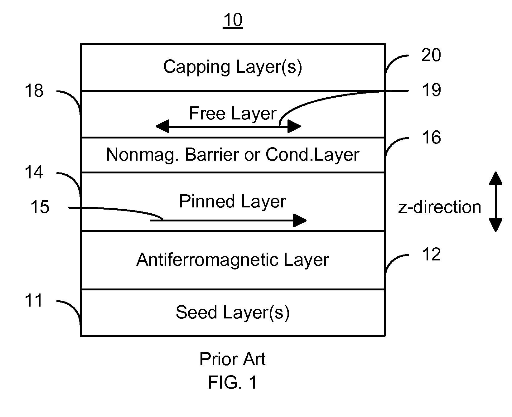
Consequently, power consumption of the MRAM using the conventional magnetic element 10 increases and the high more reliability issues may be encountered.
Such a write scheme may thus be unsuitable for use at higher densities.
This high bias current is undesirable for a number of reasons.
A high bias current implies that the magnetic memory using the conventional magnetic element 10 has a higher power consumption during writing.
On the other hand, reducing the magnetization Ms results in the decrease of shape anisotropy and magnetic energy barrier which leads to the thermally-activated loss of the stored information.
Consequently, without more, a reduction of the magnetization is not desirable for reducing the switching current of the conventional magnetic element 10.

Method used


Image

  • Method and system for providing domain wall assisted switching of magnetic elements and magnetic memories using such magnetic elements
  • Method and system for providing domain wall assisted switching of magnetic elements and magnetic memories using such magnetic elements
  • Method and system for providing domain wall assisted switching of magnetic elements and magnetic memories using such magnetic elements

Examples


Embodiment Construction

[0025]The method and system relate to magnetic memories. The following description is presented to enable one of ordinary skill in the art to make and use the method and system and is provided in the context of a patent application and its requirements. Various modifications to the embodiments and the generic principles and features described herein will be readily apparent to those skilled in the art. Thus, the method and system are not intended to be limited to the embodiments shown, but is to be accorded the widest scope consistent with the principles and features described herein.

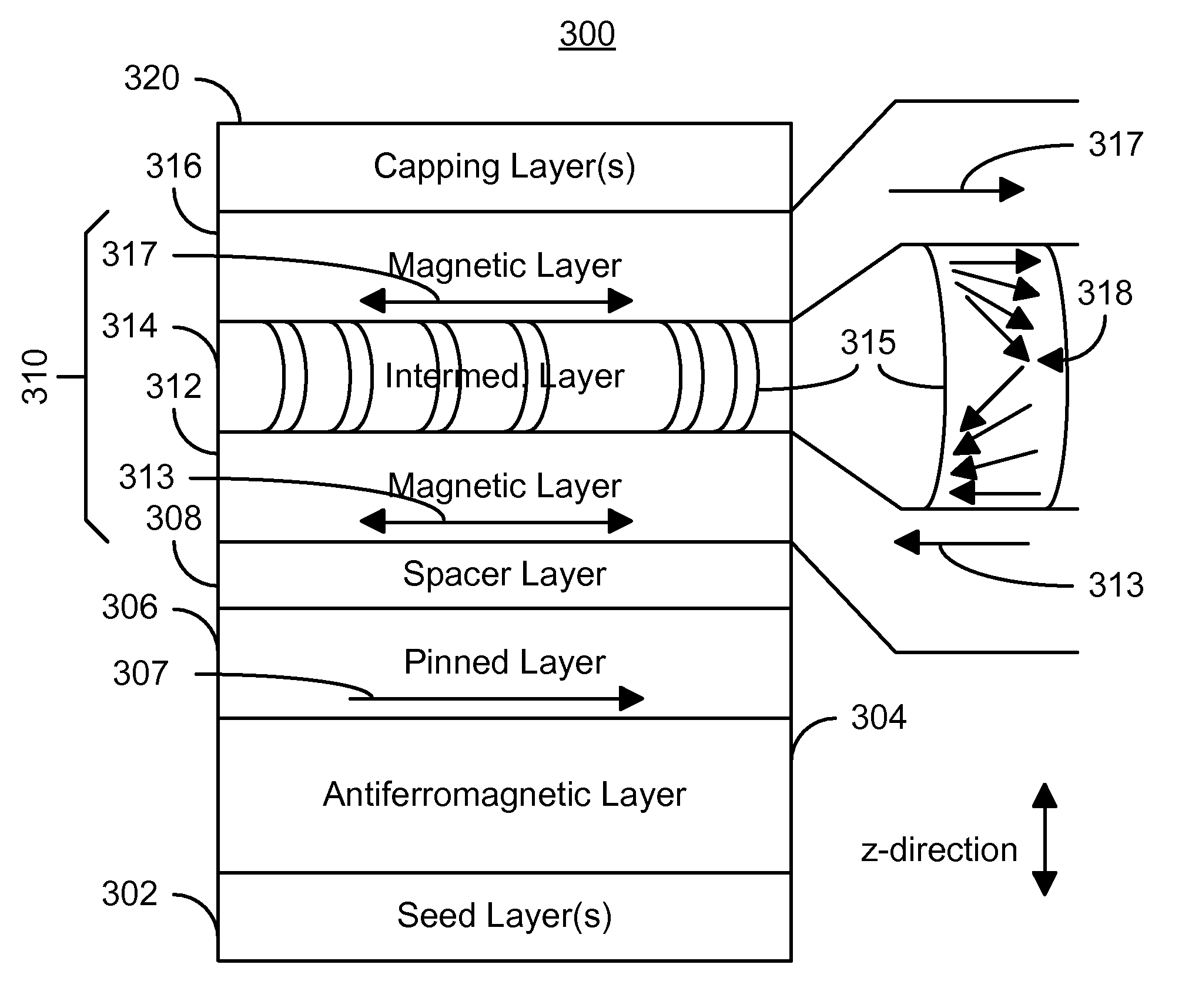
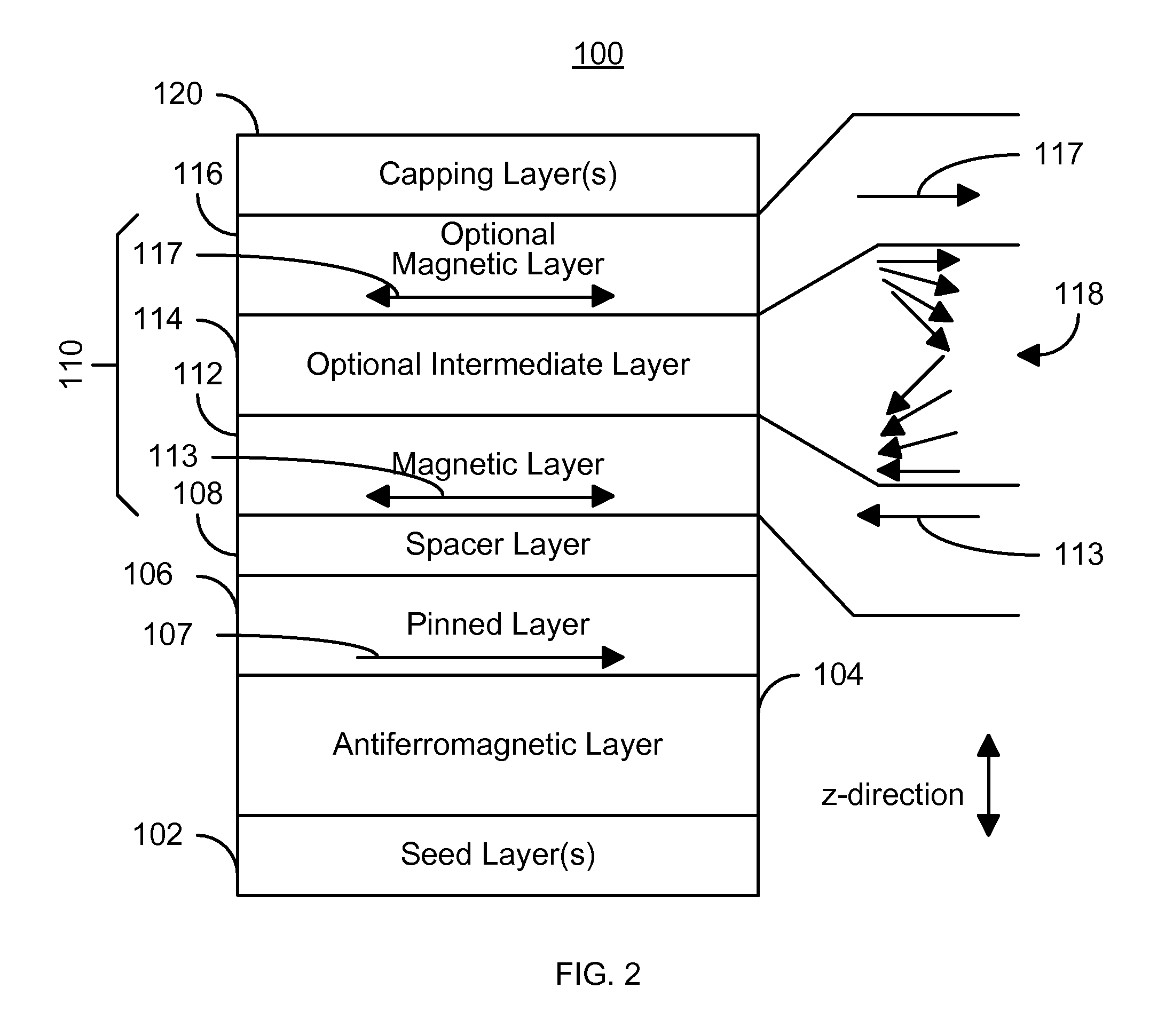
[0026]A method and system for providing a magnetic element are disclosed. The magnetic element includes a pinned layer, a spacer layer, and a free layer. The spacer layer is nonferromagnetic and resides between the pinned layer and the free layer. The free layer includes a first magnetic layer and at least one of a second magnetic layer and an intermediate layer. The intermediate layer would reside betw...


PUM


Abstract

A method and system for providing a magnetic element is described. The magnetic element includes a pinned layer, a spacer layer, and a free layer. The spacer layer is nonferromagnetic and resides between the pinned layer and the free layer. The free layer includes a first magnetic layer and at least one of a second magnetic layer and an intermediate layer. The intermediate layer would reside between the first and second magnetic layers. The free layer also includes at least one domain wall therein during switching. In addition, the magnetic element is configured to allow the free layer to be switched at least in part due to spin transfer when a write current is passed through the magnetic element.

Description

BACKGROUND OF THE INVENTION[0001]Magnetic memories, particularly magnetic random access memories (MRAMs), have drawn increasing interest due to their potential for high read / write speed, excellent endurance, non-volatility and low power consumption during operation. An MRAM can store information utilizing magnetic materials as an information recording medium. Typically, a conventional magnetic element is used for storing data in such magnetic memories.[0002]FIG. 1 depicts a conventional magnetic element 10, which may be a conventional magnetic tunneling junction (MTJ) or a conventional spin valve. The conventional magnetic element 10 may be used in a conventional magnetic memory. The conventional MTJ 10 typically resides on a substrate (not shown), uses seed layer(s) 11 and includes a conventional antiferromagnetic (AFM) layer 12, a conventional pinned layer 14, a conventional barrier layer 16, a conventional free layer 18, and a conventional capping layer 20. The conventional pinne...

Claims


Application Information

Patent Timeline
IPC IPC(8): G11C11/15
CPCG11C11/16G11C11/161G11C11/1675
Inventor LI, ZHANJIEWANG, SHENGYUAN
Owner SAMSUNG SEMICON
Learn More