Techniques for debugging hard intellectual property blocks

a technology of intellectual property blocks and debugging techniques, applied in the direction of computation using denominational number representation, pulse technique, instruments, etc., can solve the problems of squandering a significant number of the limited i/o pins of the hip block, difficult hardware debugging of the hip block embedded in the pld, and many of the dedicated i/o pins become unnecessary

Inactive Publication Date: 2009-01-20
ALTERA CORP
View PDF4 Cites 4 Cited by
  • Summary
  • Abstract
  • Description
  • Claims
  • Application Information

AI Technical Summary

Benefits of technology

[0007]According to one embodiment of the present invention, the HIP block can be functionally partitioned into a receive (RX) side and a transmit (TX) side. Each side may then implement one or more state machines with selected internal signals as inputs. Also, state information for each side can be captu...

Problems solved by technology

A HIP block embedded in PLD is very difficult to hardware debug as internal signals of the HIP block cannot be directly probed.
However, many of these dedicated I/O p...

Method used


Image

  • Techniques for debugging hard intellectual property blocks
  • Techniques for debugging hard intellectual property blocks
  • Techniques for debugging hard intellectual property blocks

Examples


Embodiment Construction

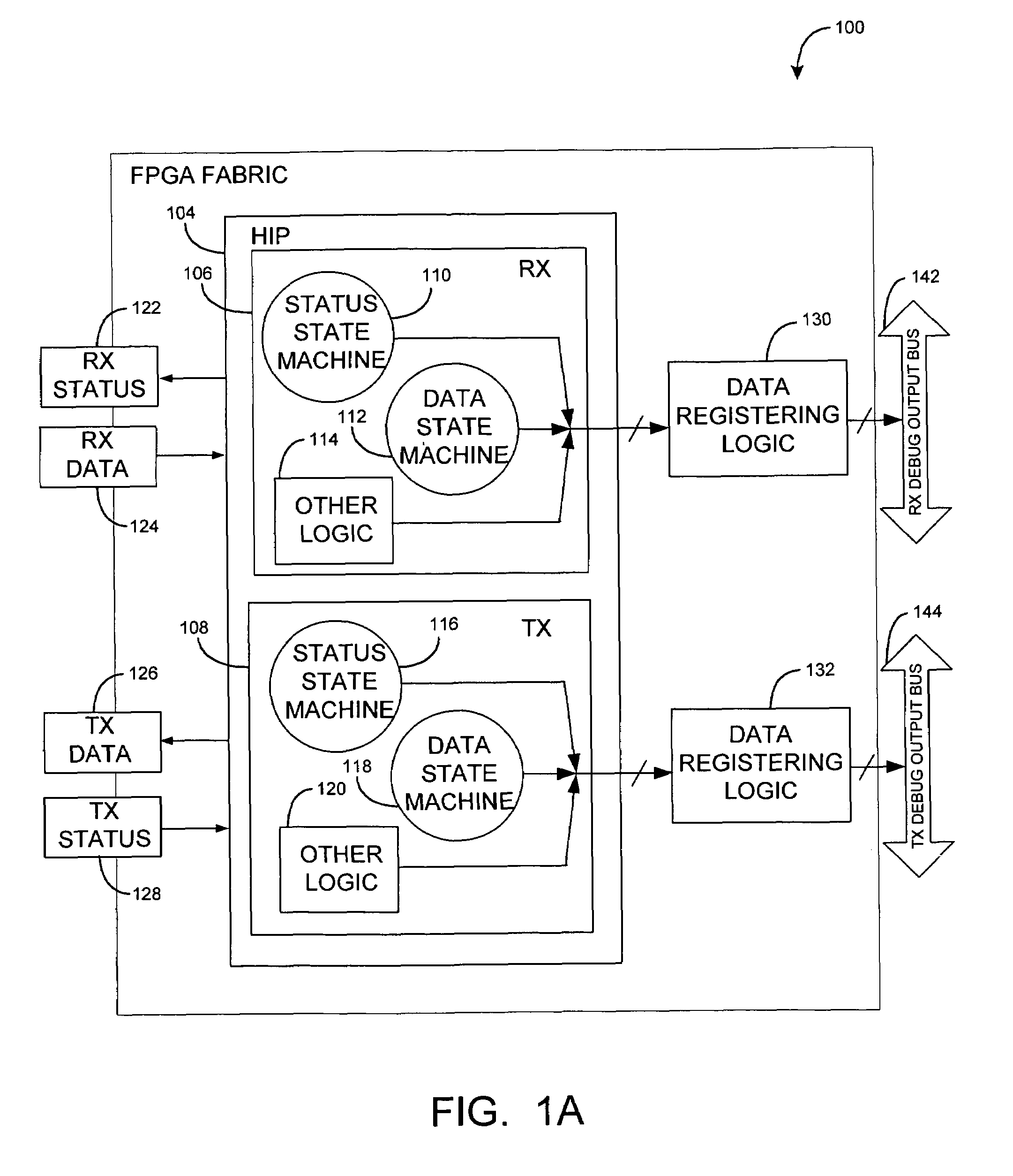
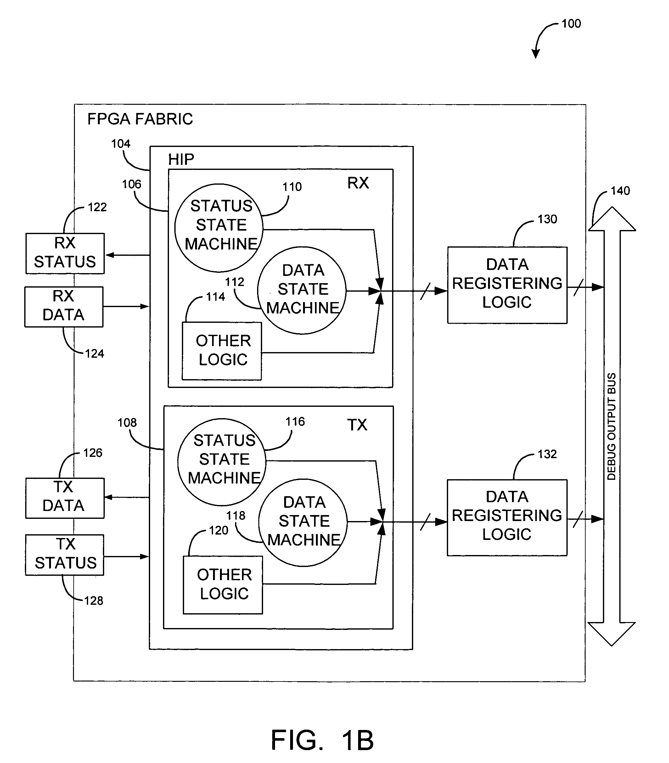
[0014]FIGS. 1A and 1B illustrate block diagrams of a programmable logic integrated circuit (IC) 100 that includes a hard intellectual property (HIP) block according to embodiments of the present invention. IC 100 is a field programmable gate array (FPGA). Although the present invention is discussed primarily in the context of programmable logic integrated circuits such as PLDs and FPGAs, it should be understood the present invention is not limited to programmable logic integrated circuits. The techniques of the present invention can also be applied to ASICs and other types of integrated circuits.

[0015]FPGA 100 includes HIP block 104 and optional data registering logic circuits 130, 132. HIP block 104 can be designed to perform any desirable functions. In a specific embodiment, HIP block 104 is configured to exchange I / O data with an external device in compliance with System Packet Interface, Level 4, Phase 2 (SPI4-2). HIP block 104 generates and receives various I / O signals, such as...


PUM


Abstract

Techniques are provided to hardware debug a programmable logic integrated circuit that includes a hardware intellectual property block (HIP). The HIP includes a logic circuit and state machine(s). The state machine outputs state machine information depending on selected signals within the logic circuit. The HIP block can also output data from a number of internal registers/flip-flops. Optional data registering logic can capture the state machine information and output it to a data bus.

Description

BACKGROUND OF THE INVENTION[0001]The present invention relates to techniques for debugging hard intellectual property blocks, and more particularly, to techniques for accessing various internal signals of a hard intellectual property block.[0002]Programmable logic devices (PLDs) are a type of programmable logic integrated circuit. Programmable logic integrated circuits can be configured to perform a variety of logical user functions. Programmable logic integrated circuits also include field programmable gate arrays (FPGAs), programmable logic arrays, configurable logic arrays, etc.[0003]PLDs typically have numerous logic blocks that can be configured to implement various combinatorial and sequential functions. The logic blocks have access to a programmable interconnect structure. The programmable interconnect structure can be programmed to interconnect the logic blocks in almost any desired configuration. Many of today's PLDs have on-chip non-programmable application specific integr...

Claims


Application Information

Patent Timeline
IPC IPC(8): G06F7/38H03K19/173
CPCG01R31/31705
Inventor WAGENINGEN, DARREN VANANG, BOON JIN
Owner ALTERA CORP
Why Eureka
Try Eureka