Flash memory device and erasing method thereof

a flash memory and memory device technology, applied in static storage, digital storage, instruments, etc., can solve the problems of long time, inability to carry out post-programming operations for selected memory cells in normal conditions, and inability to carry out post-programming operations in normal conditions, etc., to shorten the whole erasing time

Inactive Publication Date: 2008-12-02
SAMSUNG ELECTRONICS CO LTD
View PDF18 Cites 69 Cited by
  • Summary
  • Abstract
  • Description
  • Claims
  • Application Information

AI Technical Summary

Benefits of technology

[0015]Exemplary embodiments of the present invention are directed to provide a flash memory device capable of shortening the whole erasing time and to provide a post-programming method thereof.
[0016]Furthermore, exemplary embodiments of the present invention are directed to provide a flash memory device and to provide a method capable of shortening the time for conducting a post-programming operation.
[0017]Exemplary embodiments of the present invention are also directed to provide a flash memory device capable of controlling the number of memory cells to be programmed at a time during a post-programming operation and a method thereof.
[0028]In an exemplary embodiment of the present invention, a flash memory device having a memory cell array with memory cells arranged in rows and columns comprises: a row decoder selecting the rows in response to a row address; a column decoder selecting the columns in response to a column address, write drivers divided into plural groups, driving the selected columns with a bit line voltage; a column address generator counting the number of post-programming operations and generating the column address and a count-up pulse signal; a row address generator configured to store reference addresses, generating the row address in response to the count-up pulse signal; and a selection circuit generating selection signals to activate the write driver groups in response to the counted value. The row address generator outputs flag information indicating a change of column selection unit whenever the row address matches one of the reference addresses. The selection circuit controls activation of the selection signals in accordance with the flag information so as to increase the number of memory cells to be post-programmed in the selected columns.

Problems solved by technology

All kinds of flash memories or EEPROMs are usually configured in a certain structure such that insulation films enclosing charge storage elements used for storing data are inevitably worn out after a specific number of operations.
If an amount of leakage current increases, the post-programming operation for selected memory cells may not be carried out in a normal condition.
By the restrictive number of memory cells that can be programmed at a time, it may take a long time in conducting the post-programming operation, resulting in an increase in the whole erasing time of the flash memory device.

Method used


Image

  • Flash memory device and erasing method thereof
  • Flash memory device and erasing method thereof
  • Flash memory device and erasing method thereof

Examples


Embodiment Construction

[0050]Exemplary embodiments of the present invention will be described below in more detail with reference to the accompanying drawings, showing a flash memory device as an exemplary embodiment for illustrating structural and operational features. The present invention may, however, be embodied in different forms and should not be constructed as limited to the exemplary embodiments set forth herein. Rather, these exemplary embodiments are provided so that this disclosure will be thorough and complete, and will fully convey the scope of the present invention to those skilled in the art. Like reference numerals refer to like elements throughout the accompanying figures.

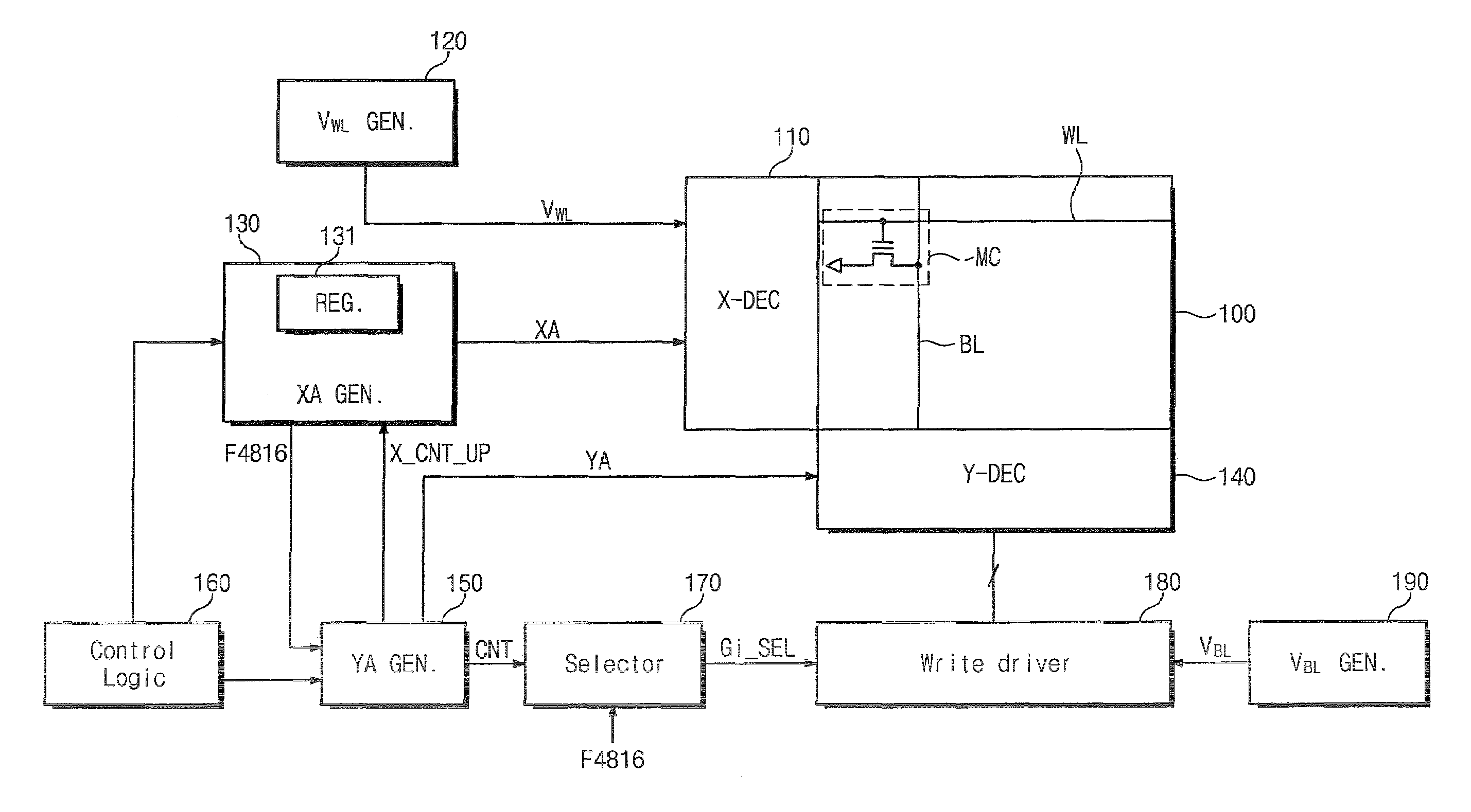
[0051]FIG. 3 is a block diagram illustrating a flash memory device in accordance with an exemplary embodiment of the present invention. This flash memory device is a NOR flash memory device for example. But, it should be understood that the present Invention is also applicable to other kinds of memory devices, for examp...


PUM


Abstract

A method of post-programming a flash memory device includes the steps of: post-programming memory cells of a selected word line in a predetermined unit; determining, after incrementing an address for selecting the next word line, whether the incremented address matches one of reference addresses; and varying the post-programming unit of the selected memory cells whenever the incremented address matches one of reference addresses.

Description

CROSS-REFERENCE TO RELATED APPLICATION[0001]This U.S. non-provisional patent application claims priority under 35 U.S.C. 517 119 of Korean Patent Application No. 2006-72193 filed on Jun. 7, 2006, the entire contents of which are hereby incorporated by reference.BACKGROUND[0002]The present disclosure relates to semiconductor memory devices and, more particularly, to flash memory devices.[0003]Flash memory devices as nonvolatile memories are kinds of electrically erasable and programmable read-only memories (EEPROMs) in which plural memory blocks are erased or written with data by one programming operation. A general EEPROM is operable with the feature that one memory block is erasable or programmable at a time. This means that the flash memories operate more rapidly and are effective in reading and writing data when systems employing such flash memory devices read and write data from and into other memory areas at the same time. All kinds of flash memories or EEPROMs are usually conf...

Claims


Application Information

Patent Timeline
Patent Type & Authority Patents(United States)
IPC IPC(8): G11C11/34G11C16/04G11C8/00
CPCG11C16/0416G11C16/3404G11C16/3409G11C16/3477G11C16/0483G11C16/08G11C16/10G11C16/3454
Inventor LEE, DOO-SUBCHOI, JONG-IN
Owner SAMSUNG ELECTRONICS CO LTD
Why Eureka
Try Eureka