Microchannel array
a microchannel array and array technology, applied in the field of microchannel arrays, can solve the problems of difficult to sufficiently cover the variation in shape, size and elasticity between cells, and the inability to collectively inject dna, and achieve the effect of increasing the cell differentiation/proliferation speed
- Summary
- Abstract
- Description
- Claims
- Application Information
AI Technical Summary
Benefits of technology
Problems solved by technology
Method used
Image
Examples
production example 1
Fabrication of Micro Chamber Array
[0093]100 through-holes having the diameter of 60 μm were formed in a 0.2-mm thick silicon substrate with the length of 20 mm and the width of 20 mm by use of a dry etching device available from Alcatel. The micro chamber array is used as Comparative Example. FIG. 9 shows the outer appearance of the micro chamber array.
production example 2
Fabrication of Microchannel Array
[0094]14 channels having the width of 80 μm, the depth of 100 μm, and the length of 5000 μm were formed in a 0.3-mm thick silicon substrate with the length of 10 mm and the width of 20 mm by use of a dry etching device available from Alcatel. The channels communicated with each other through the grooves, and then a through-hole having the diameter of 3 mm was formed in the groove through sand blasting. Then, an acrylic substrate having the same size as that of the silicon substrate was brought into contact with the silicon substrate to complete a microchannel array. FIG. 10 is an outer appearance of the microchannel array.
production example 3
Coaxial Microchannel Array A
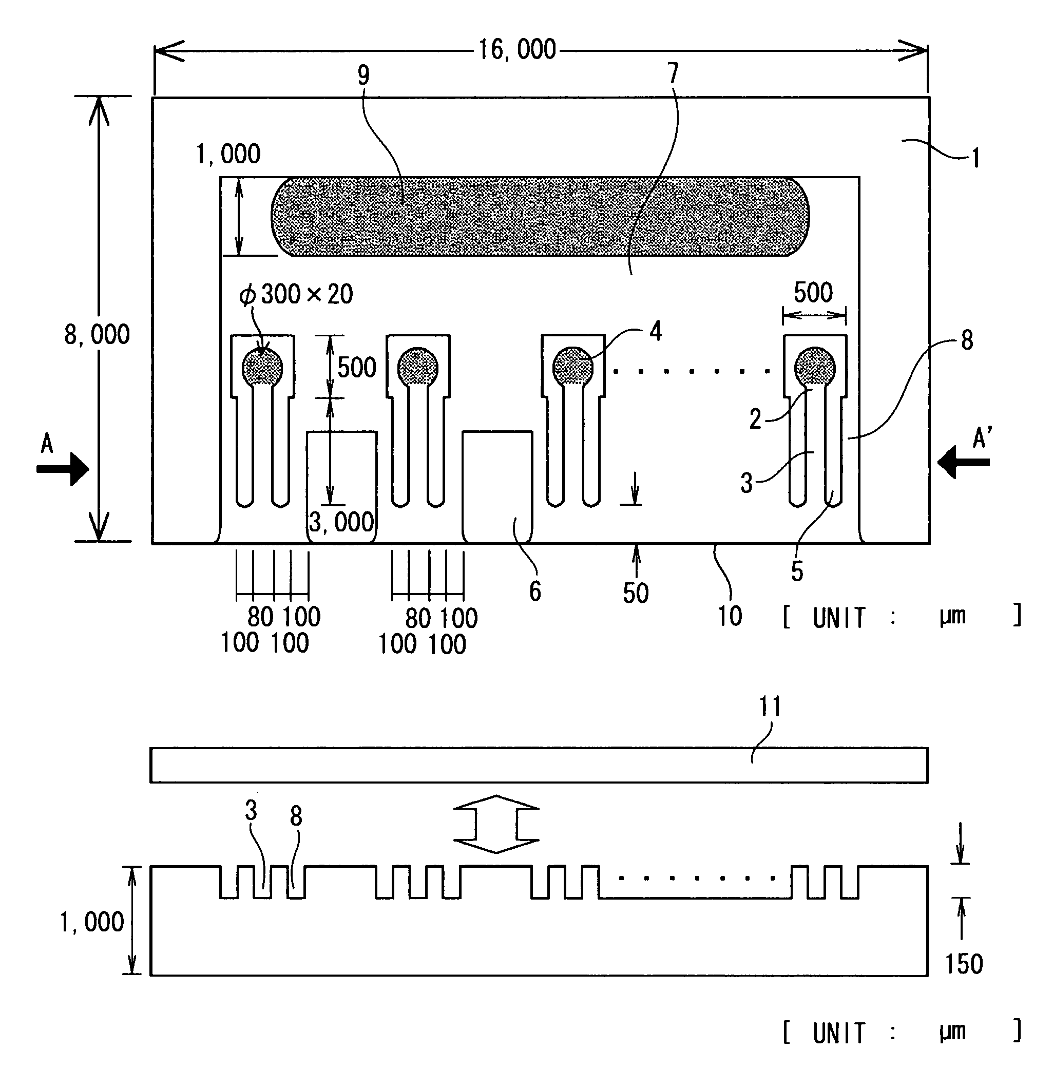
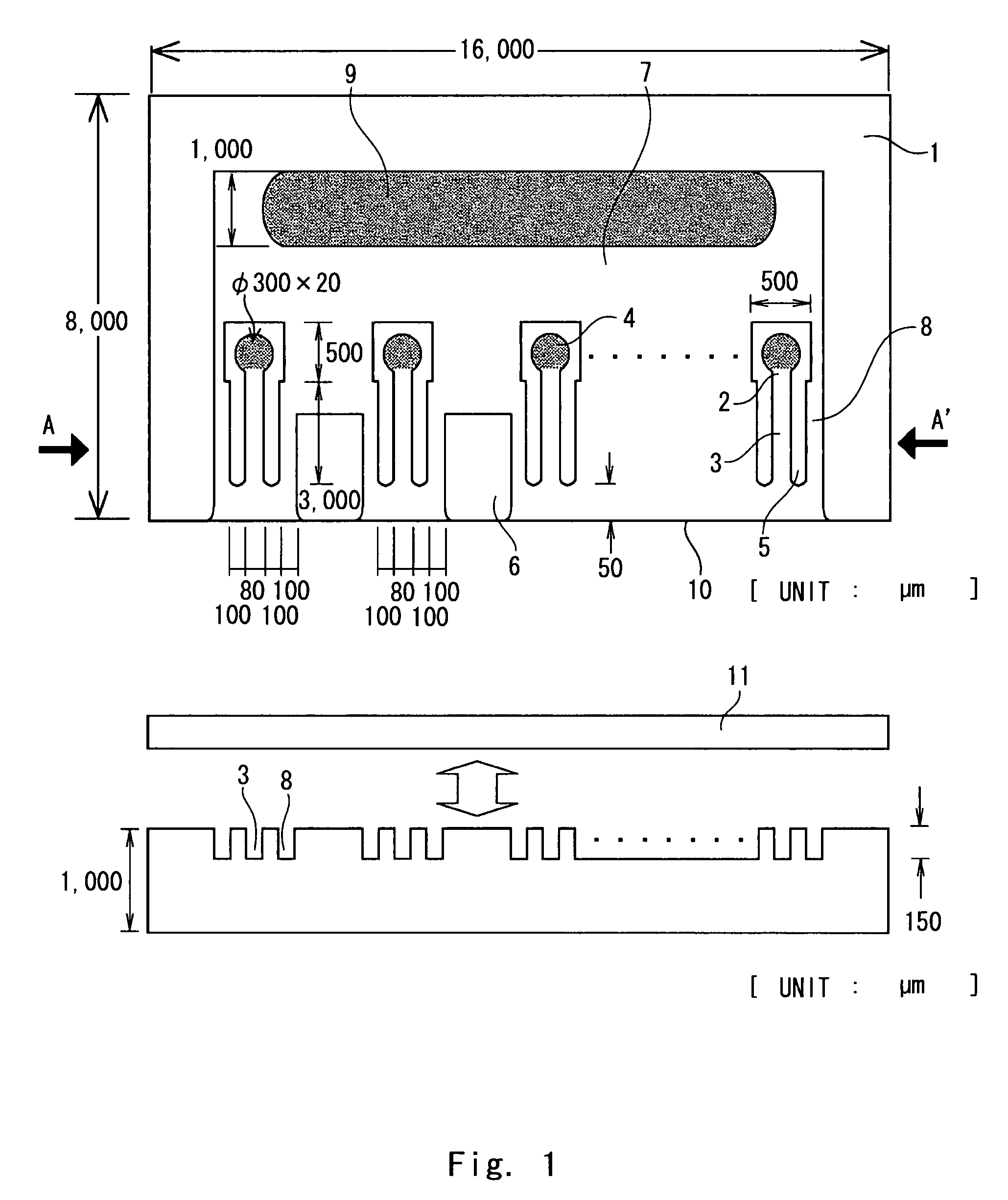
[0095]First, a resist pattern was formed on a glass plate through photolithography, and the resist pattern was subjected to plating to manufacture the metal structure. Next, the metal structure was used as a mould, and an acrylic resin (PARAPET G-HS) available from Kuraray was used as a material. A first substrate of a coaxial microchannel array A was manufactured through the injection-molding. Further, the through-hole (second through-hole 4) having the diameter of 0.3 mm was formed for sucking a cell on the substrate with a machining center. Finally, an acrylic substrate (second substrate) having substantially the same as that of the acrylic substrate was brought into close contact with the substrate to complete a coaxial microchannel array A of FIG. 1.
[0096]A shape of the coaxial microchannel array A has 20 microchannel pairs on a substrate having the width of 16 mm, the length of 8 mm, and the thickness of 1.0 mm. Each microchannel includes a first gr...
PUM
| Property | Measurement | Unit |
|---|---|---|
| width | aaaaa | aaaaa |
| contact angle | aaaaa | aaaaa |
| contact angle | aaaaa | aaaaa |
Abstract
Description
Claims
Application Information
 - R&D
- Intellectual Property
- Life Sciences
- Materials
- Tech Scout
- Unparalleled Data Quality
- Higher Quality Content
- 60% Fewer Hallucinations
Browse by: Latest US Patents, China's latest patents, Technical Efficacy Thesaurus, Application Domain, Technology Topic, Popular Technical Reports.
© 2025 PatSnap. All rights reserved.Legal|Privacy policy|Modern Slavery Act Transparency Statement|Sitemap|About US| Contact US: help@patsnap.com


