Method of manufacturing a semiconductor device by using a matrix frame

a manufacturing method and semiconductor technology, applied in semiconductor devices, semiconductor/solid-state device details, electrical devices, etc., can solve the problems of difficult to remove the flash and large time consumption of the dividing step

Inactive Publication Date: 2008-07-22
LAPIS SEMICON CO LTD
View PDF12 Cites 4 Cited by
  • Summary
  • Abstract
  • Description
  • Claims
  • Application Information

AI Technical Summary

Benefits of technology

[0015]A method of manufacturing a semiconductor device according to preferred embodiments of the present invention will be explained hereinafter with reference to the accompanying figures. In order to simplify the explanation, like elements are given like or corresponding reference numerals. Dual explanations of the same elements are avoided.

Problems solved by technology

It is difficult to remove the flash, and an additional step for removing the flash is needed.
Therefore, the dividing step requires a lot of time.

Method used


Image

  • Method of manufacturing a semiconductor device by using a matrix frame
  • Method of manufacturing a semiconductor device by using a matrix frame
  • Method of manufacturing a semiconductor device by using a matrix frame

Examples


Embodiment Construction

[0015]A method of manufacturing a semiconductor device according to preferred embodiments of the present invention will be explained hereinafter with reference to the accompanying figures. In order to simplify the explanation, like elements are given like or corresponding reference numerals. Dual explanations of the same elements are avoided.

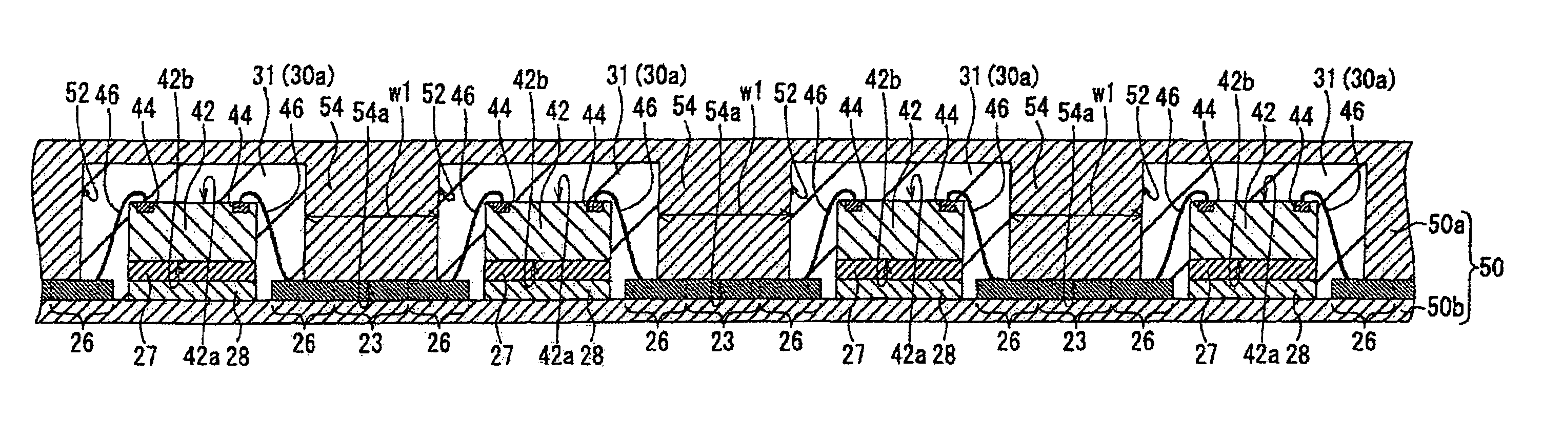
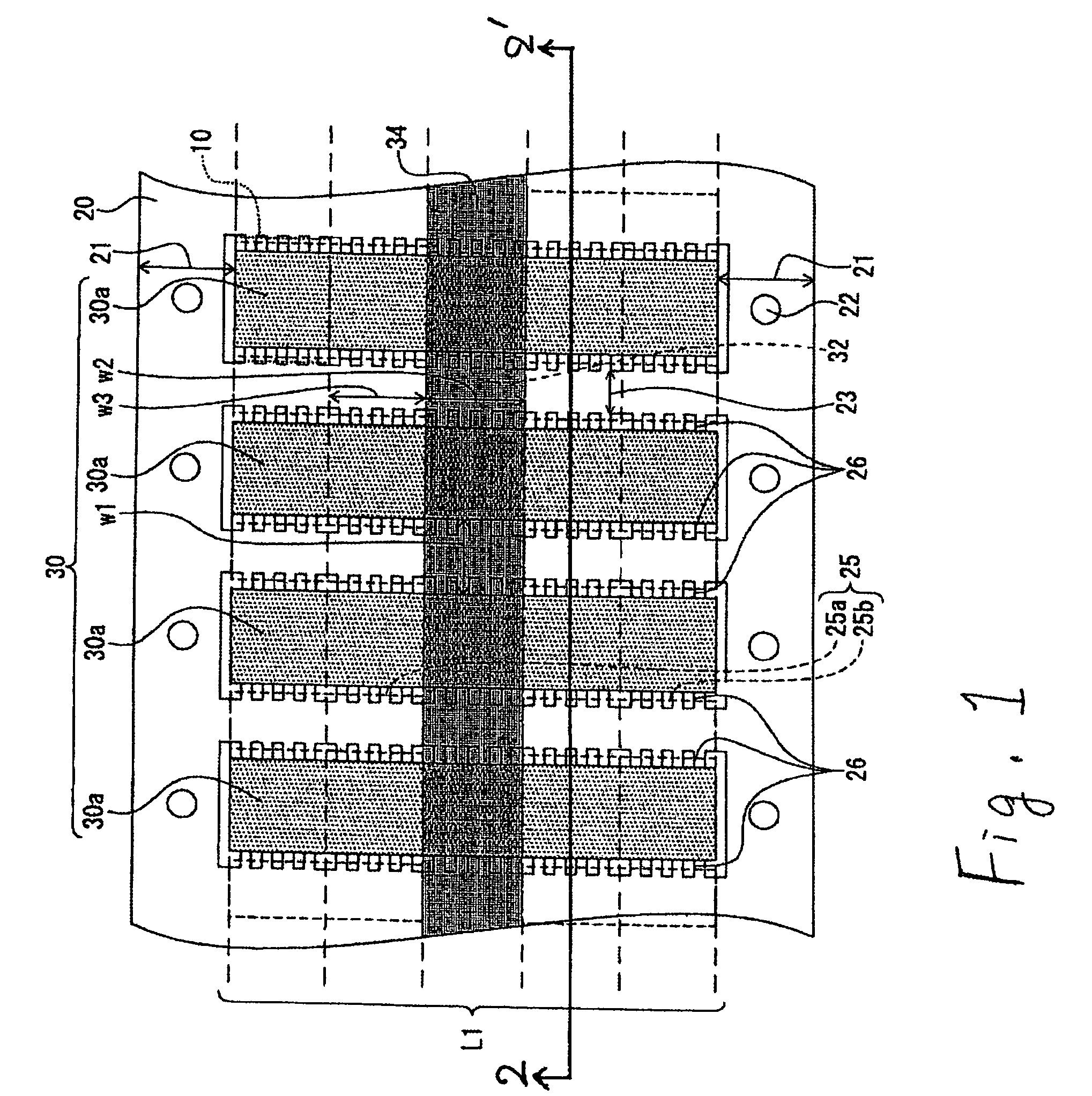
[0016]Initially, a structure of a lead frame 20 of the present invention is described by referring to FIG. 4. The lead frame 20 is made from a metal plate such as copper and has a rectangular configuration. The lead frame 20 includes a plurality of die pads 28, a frame portion 21, supporting leads 29, connecting portions 23, and inner leads 26. Each of the part including the die pads 28, supporting leads 29, connecting portion 23, and inner leads 26 are formed by a punching method or by a etching method from the metal plate.

[0017]The die pads 28 are arranged in a matrix with a distance provided between each of the die pads 28. Each of the die pa...


PUM


Abstract

A method of manufacturing a semiconductor device includes providing a matrix frame which includes a plurality of die pads, mounting a semiconductor chip on the respective die pads, and sealing the semiconductor chip in blocks. After the semiconductor chip is sealed by the sealing resin, inner leads which are extended from the sealing resin are punched by a punching blade. Then, the block is diced to individual semiconductor devices by a rotary blade.

Description

CROSS REFERENCE TO RELATED APPLICATION[0001]A claim of priority under 35 U.S.C. §119 is made to Japanese Patent Application No. 2003-430438, filed Dec. 25, 2003, which is herein incorporated by reference in its entirety for all purposes.BACKGROUND OF THE INVENTION[0002]1. Field of the Invention[0003]The present invention relates to a method of manufacturing a semiconductor device which has a sealing resin.[0004]2. Description of the Related Art[0005]A technique of manufacturing a semiconductor device using a matrix frame is disclosed in reference 1: Japanese Patent Laid-Open No. 2000-124239. The matrix frame which is disclosed in reference 1 includes a plurality of die pads which are arranged in a matrix. A semiconductor chip is mounted on the respective die pads. A couple of the semiconductor chips and the die pads are grouped and sealed in groups by a sealing resin. Such technique may be called a block molding method.[0006]A reference 2: Japanese Patent Laid-Open No. 2002-43344 di...

Claims


Application Information

Patent Timeline
Patent Type & Authority Patents(United States)
IPC IPC(8): H01L21/46H01L21/30H01L21/301H01L21/78H01L21/44H01L21/56H01L21/48H01L21/50H01L23/31H01L23/495
CPCH01L21/4842H01L21/565H01L23/3107H01L24/97H01L21/561H01L2924/01005H01L23/49513H01L2224/32245H01L2224/48091H01L2224/48247H01L2224/73265H01L2224/97H01L2924/01029H01L2924/01082H01L24/48H01L2924/01006H01L2924/01033H01L2924/07802H01L2924/00014H01L2224/83H01L2224/85H01L2924/00012H01L2924/00H01L24/73H01L2924/181
Inventor YAMADA, ETSUO
Owner LAPIS SEMICON CO LTD
Why Eureka
Try Eureka