Method of manufacturing semiconductor device

a manufacturing method and semiconductor technology, applied in the direction of semiconductor devices, basic electric elements, electrical appliances, etc., can solve the problems of inadvertent increase in the thickness of the oxide layer formed in a subsequent process, increase in the thickness deterioration of the quality of the oxide layer, etc., to achieve the effect of suppressing the occurrence of recoiled oxygen

Active Publication Date: 2008-04-22
MARVELL ASIA PTE LTD +1
View PDF7 Cites 4 Cited by
  • Summary
  • Abstract
  • Description
  • Claims
  • Application Information

AI Technical Summary

Benefits of technology

[0008]In order to solve the aforementioned problems, an object of the present invention is to provide a method of manufacturing a semiconductor device capable of forming a thin high-quality gate oxide layer by suppressing occurrence of recoiled oxygen due to ion implanting.

Problems solved by technology

However, in the above cases, there is a problem in that recoiled oxygen is induced by the ion implanting process, so that the thickness of the oxide layer formed in a subsequent process may inadvertently increase.
Therefore, the thickness of the oxide layer may increase and the quality thereof may deteriorate.

Method used


Image

  • Method of manufacturing semiconductor device
  • Method of manufacturing semiconductor device
  • Method of manufacturing semiconductor device

Examples


Embodiment Construction

[0015]Now, exemplary embodiments of the present invention will be described with reference to the attached drawings. However, the present invention can be embodied in various modifications and thus is not limited to the embodiments described below.

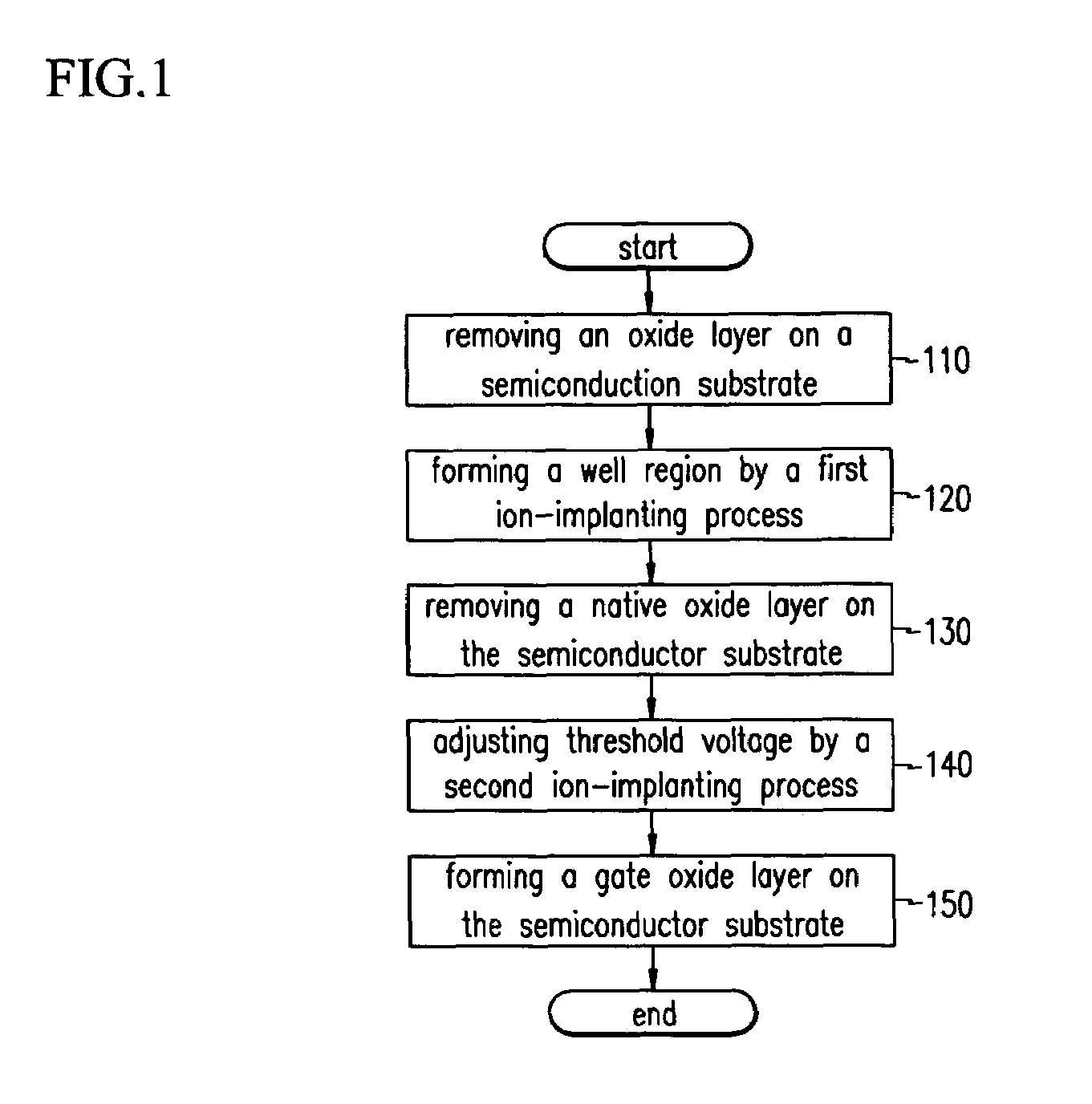
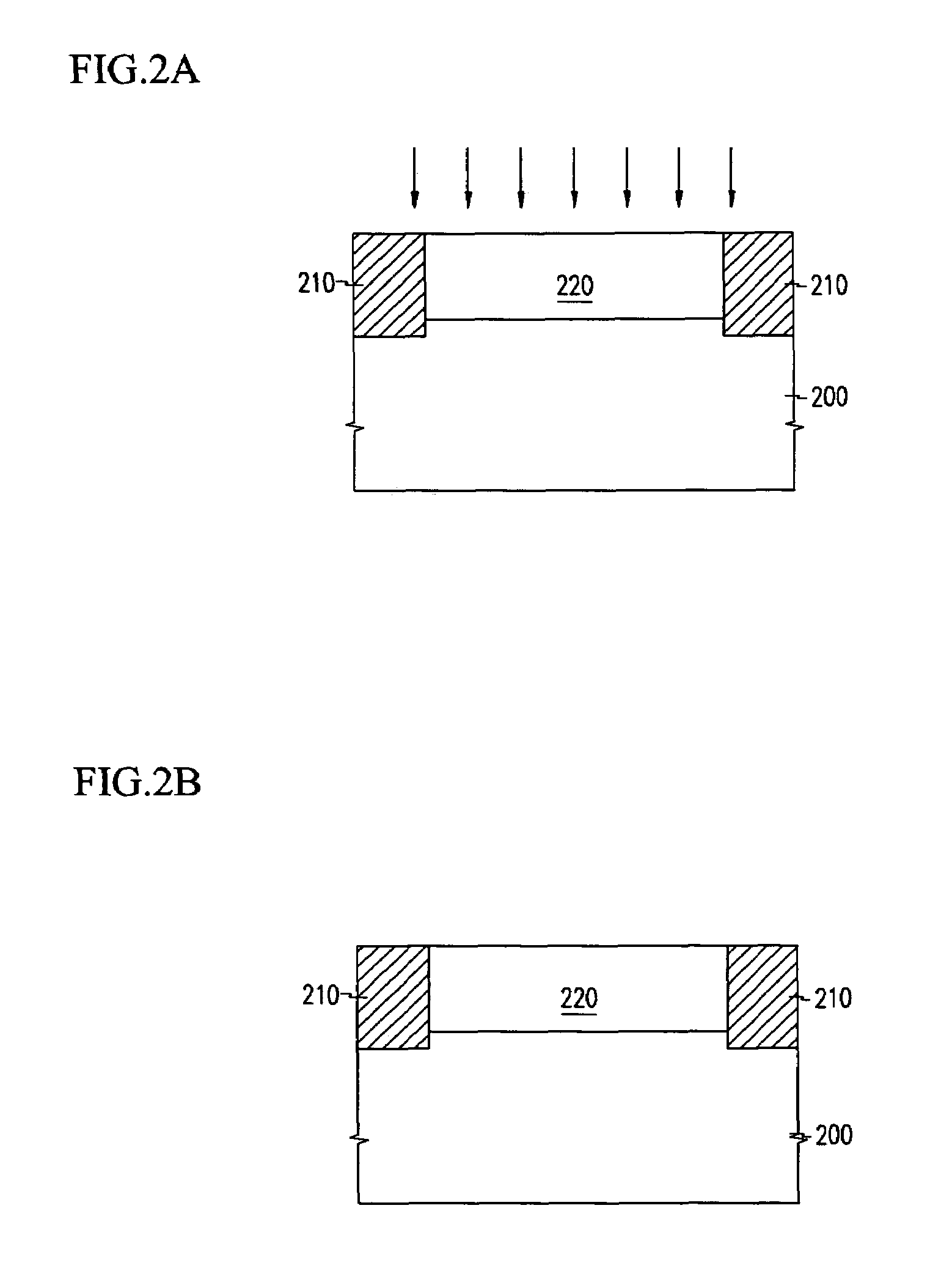
[0016]FIG. 1 is a flowchart showing steps of a method of forming a gate oxide layer according to the present invention, and FIGS. 2A to 2D are cross sectional views for explaining the steps of FIG. 1.

[0017]Referring to FIG. 2A, the entirety of an oxide layer (not shown) on semiconductor substrate 200 where an active region is defined by isolation structures 210 is removed (step 110 in FIG. 1). The oxide layer removed in step 110 is generally used in forming isolation structures 210 and is sometimes known as a “pad oxide.” Next, as indicated with arrows in FIG. 2A, a first ion implanting process is performed using a predetermined mask pattern (not shown) to form a well region 220 in the active region of the semiconductor substrate 200 (see ...


PUM


Abstract

Provided is a method of manufacturing a semiconductor device capable of forming a thin high-quality gate oxide layer by suppressing occurrence of recoiled oxygen due to ion implanting. The method of manufacturing a semiconductor device includes steps of: removing an oxide layer from a semiconductor substrate; forming a well region in the substrate by performing a first ion implanting process; removing a native oxide layer from the substrate; adjusting a threshold voltage by performing a second ion implanting process on the substrate; and forming a gate oxide layer on the substrate.

Description

BACKGROUND OF THE INVENTION[0001](a) Field of the Invention[0002]The present invention relates to a method of manufacturing a semiconductor device, and more particularly, to a method of forming a gate oxide layer of a semiconductor.[0003](b) Description of the Related Art[0004]Oxide layers have been used as a useful insulating layer in technologies for manufacturing semiconductor devices. The oxide layers such as gate insulating layers of MOS transistor devices have been used as an insulating structure for blocking carriers and providing electrical insulation between elements in the semiconductor devices. In addition, the oxide layers have been used as a field structure such as a LOCOS and a trench isolation structure for inhibiting the inadvertent formation of conductive paths between devices in an integrated circuit. In addition, the oxide layers have been used as a diffusion barrier for selectively doping or diffusing a predetermined ion or impurity on a silicon substrate in an i...

Claims


Application Information

Patent Timeline
Patent Type & Authority Patents(United States)
IPC IPC(8): H01L21/336H01L21/76H01L21/28H01L29/10
CPCH01L29/105H01L21/28167H01L21/18
Inventor KIM, HAK-DONG
Owner MARVELL ASIA PTE LTD
Why Eureka
Try Eureka