
Photonic interconnections that include optical transmission paths for transmitting optical signals

a technology of optical transmission paths and photonic interconnections, applied in the field of integrated circuit interconnections, can solve the problems of long relative time needed to traverse multiplexed circuit paths, the inability to take full advantage of the high-speed performance of nanoscale components, and the limitations of microscale circuits

Active Publication Date: 2008-04-15
HEWLETT-PACKARD ENTERPRISE DEV LP
View PDF3 Cites 12 Cited by
  • Summary
  • Abstract
  • Description
  • Claims
  • Application Information

AI Technical Summary

Benefits of technology

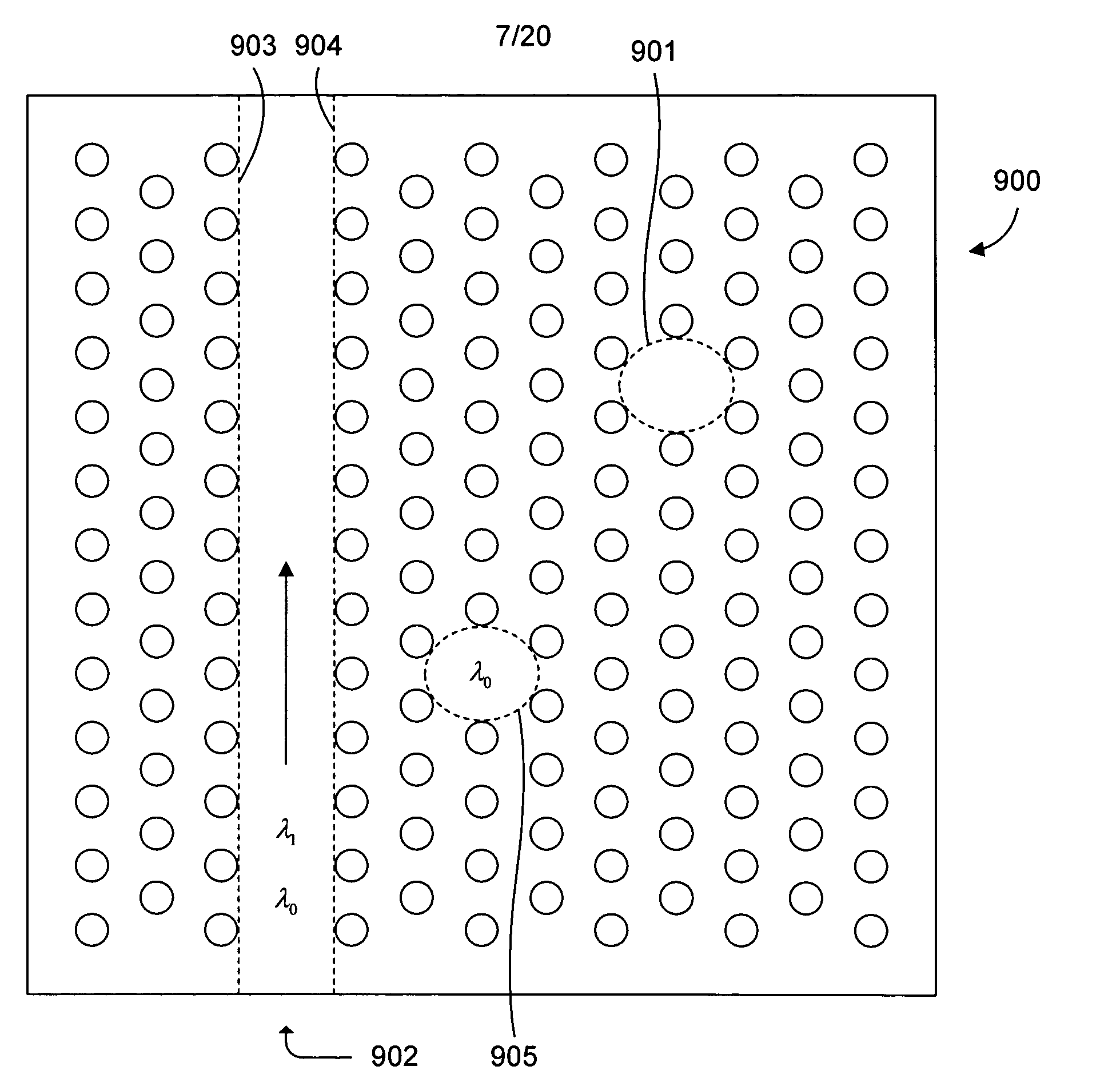
The present invention provides photonic interconnection architectures that can connect microdevices quickly. One embodiment uses an optical signal to synchronize the operation of components within a computing device. The optical signal is transmitted through a photonic crystal with filters that extract specific frequency channels carrying a clock signal. The filters are then converted into electrical signals by photodetectors, which are then used by the components of the computing device. This allows for faster and more synchronized operation.

Problems solved by technology

However, nanoelectronic tiles are subject to many of the same limitations associated with microscale circuits.
As a result, the relative amount of time needed to traverse the multiplexed circuit paths become too long to take full advantage of the high-speed performance offered by nanoscale components.
Furthermore, the information carrying capacity of nanoscale electrical interconnections carrying data, power and clock signals is lower that microscale equivalents, and closely spaced signal lines cannot pass high speed signals without creating interference between adjacent signal lines, such as inducing currents in adjacent signal lines.
Nanoscale implementations of computer components, therefore, may fail to take full advantage of the miniaturization offered by mosaics of nanoelectronic tiles, because of limitations in the degree to which the sizes of the interconnections can be decreased constrain the overall size decreases that can be achieved by using nanoscale components.

Method used

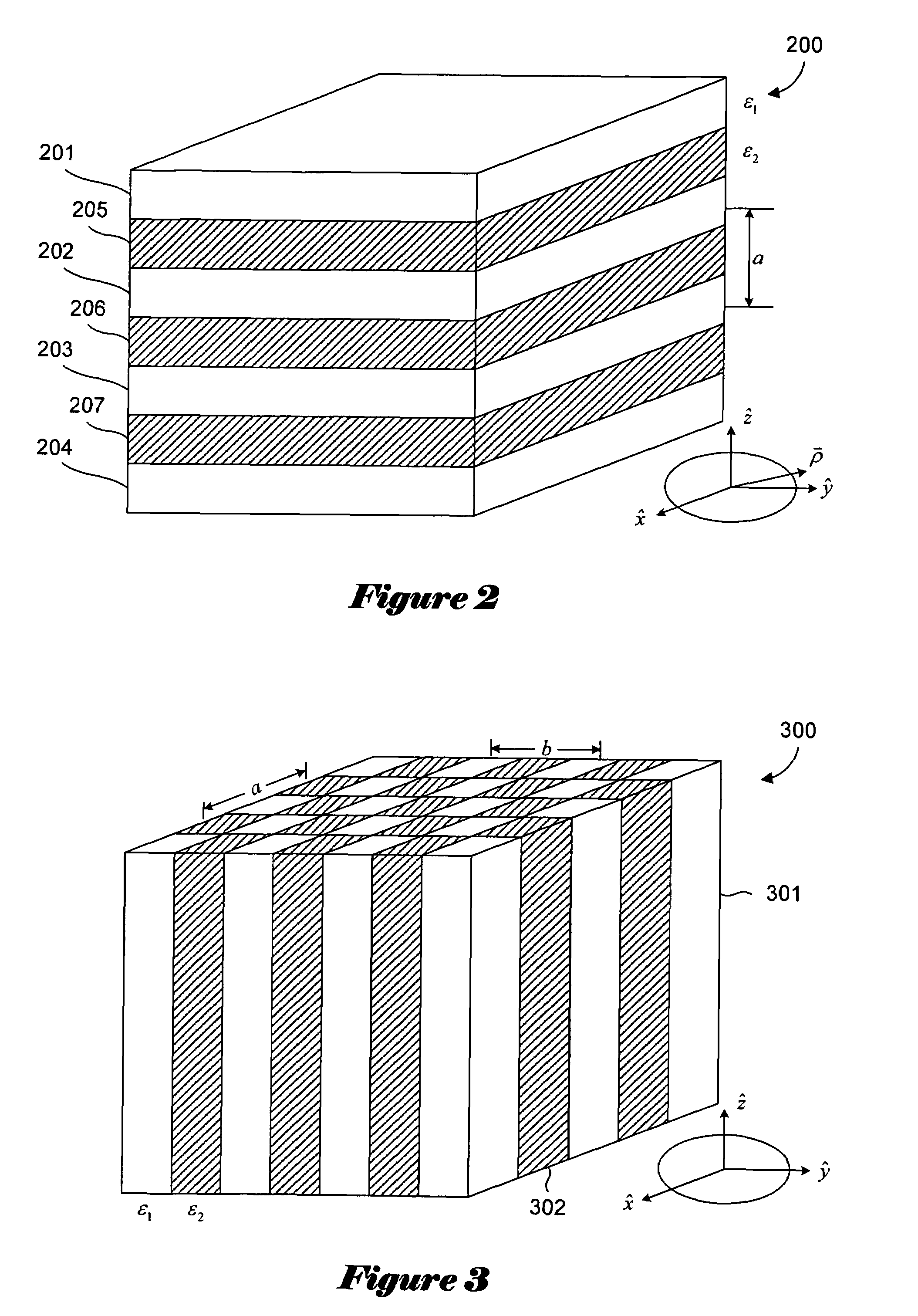

Image

  • Photonic interconnections that include optical transmission paths for transmitting optical signals
  • Photonic interconnections that include optical transmission paths for transmitting optical signals
  • Photonic interconnections that include optical transmission paths for transmitting optical signals

Examples


Embodiment Construction

[0074]In one embodiment of the present invention, a large number of relatively high capacitance electrical signal line interconnections needed to transmit address signals, clock signals, and data signals within a computer system are replaced with a relatively small number of high-speed photonic interconnections. In certain embodiments of the present invention, the photonic interconnections are composed of one or more waveguides that confine and direct the transmission of electromagnetic radiation (“ER”). The waveguides can be coaxial cables, optical fibers, line defects in photonic crystals, or any other medium that can be used to simultaneously transmit a number of different frequency channels.

[0075]FIGS. 12A-12C illustrate photonic interconnection architectures for ICs, each representing an embodiment of the present invention. FIG. 12A illustrates a first exemplary IC photonic interconnection architecture. CPU 1200 accesses circuit units 1230-1233 via converter 1220. Circuit units...


PUM

PropertyMeasurementUnit
dielectric constant ε2aaaaaaaaaa
dielectric constantaaaaaaaaaa

Abstract

Various embodiments of the present invention are directed to photonic interconnection architectures that provide high-speed interconnections of microscale or nanoscale devices. In one embodiment of the present invention, a photonic interconnection for interconnecting and synchronizing operation of components within a computing device comprises an optical transmission path for transmitting a number of independent frequency channels within an optical signal provided by an optical signal source. The photonic crystal may include one or more filters located near the waveguide for extracting specific frequency channels transmitted by the waveguide, the frequency channel including one or more frequency channels carrying a clock signal. One or more photodetectors positioned near the one or more filters convert the extracted frequency channels into electrical signals for use by one or more components of the computing device, the electrical signals including one or more clock signals for synchronizing operation of the one or more components.

Description

CROSS-REFERENCE TO RELATED APPLICATION[0001]This application is a continuation-in-part of U.S. application Ser. No. 10 / 684,278, filed Oct. 11, 2003, which was published as U.S. Publication No. 2005 / 0078902, published Apr. 14, 2005.TECHNICAL FIELD[0002]The present invention relates to integrated circuit interconnections, and, in particular, to photonic interconnections that include optical transmission paths for transmitting data and clock signals through an optical medium within a computing device.BACKGROUND OF THE INVENTION[0003]Recent developments in integrated circuit (“IC”) technology have shown remarkable promise in reducing the size of logic and memory circuits from microscale dimensions to nanoscale dimensions. Nanoscale electrical circuits, also called “nanoelectronic tiles,” can be electronically interconnected to configure larger circuit elements called “mosaics.” As a result, it may be assumed that IC component density can be significantly increased by employing mosaics o...

Claims


Application Information

Patent Timeline
Patent Type & Authority Patents(United States)
IPC IPC(8): G02B6/12G02B6/28G02B6/35G02B6/122G02B6/34G02B6/43G02F1/01G11C13/04H04B10/00H04B10/43
CPCB82Y20/00G02B6/12007G02B6/1225H04B10/801G02F1/01G02B6/43G02F2202/32G02F2203/585G02B6/34G11C13/04H04B10/00
Inventor BEAUSOLEIL, RAYWU, WEIWANG, SHIH-YUANSPILLANE, SEAN
Owner HEWLETT-PACKARD ENTERPRISE DEV LP
Learn More