Reconfigurable filter node for an adaptive computing machine
a computing machine and reconfigurable technology, applied in the field of digital processing architectures, can solve the problems of consuming significantly more power compared with other types of devices, requiring significant processing resources for microprocessors and dsps, and comparatively small amount of processing resources devoted to actual algorithmic operations
- Summary
- Abstract
- Description
- Claims
- Application Information
AI Technical Summary
Problems solved by technology
Method used
Image
Examples
embodiment 100
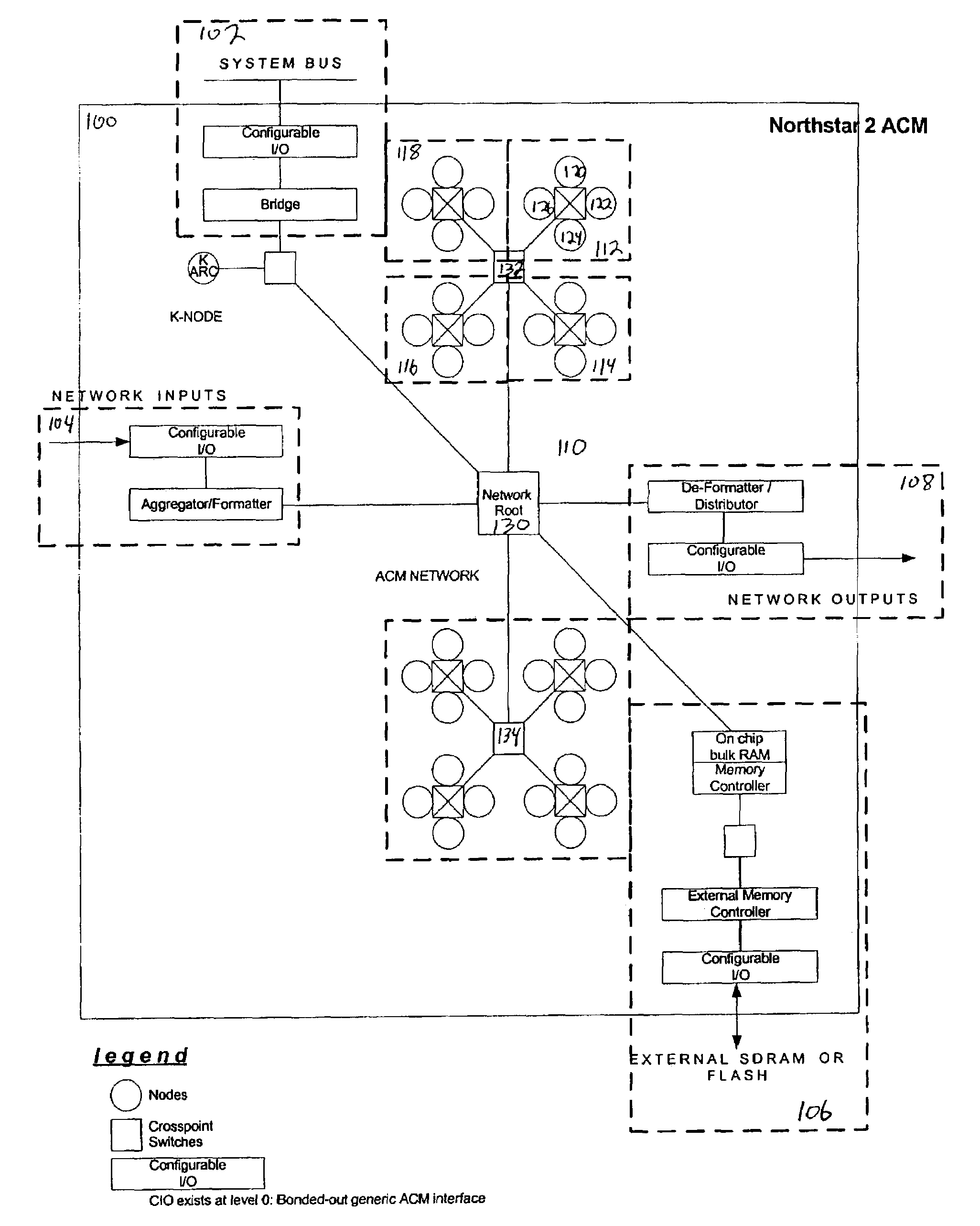
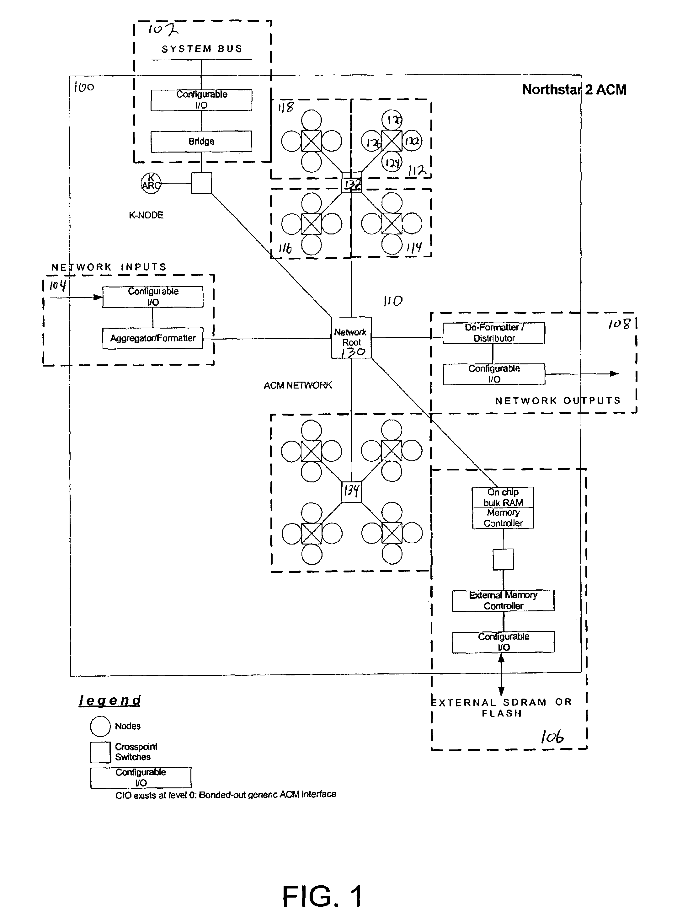
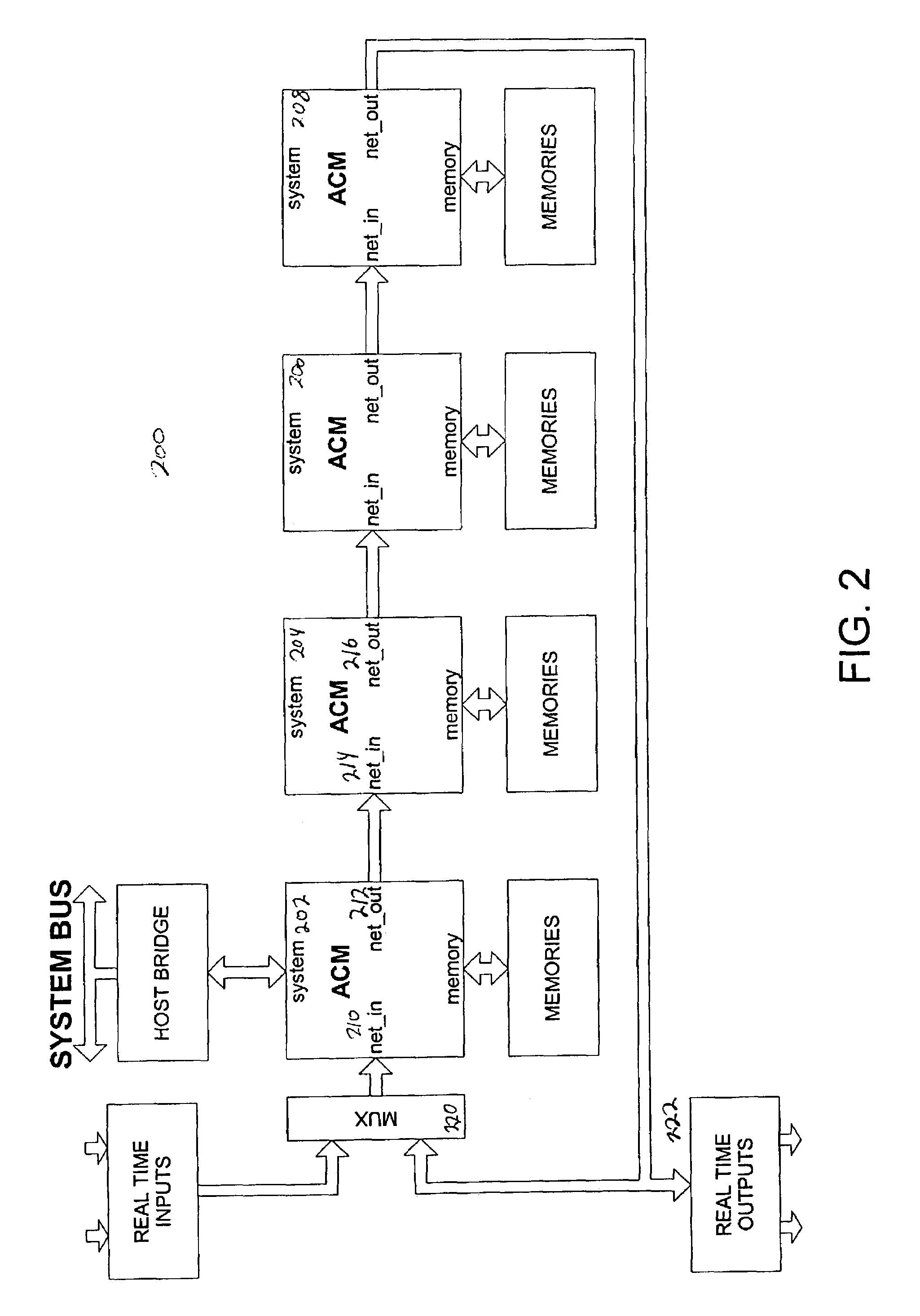
[0056]In general, the ACE architecture includes a plurality of heterogeneous computational elements coupled together via a programmable interconnection network. FIG. 1 illustrates an embodiment 100 of an ACE device. In this embodiment, the ACE device is realized on a single integrated circuit. A system bus interface 102 is provided for communication with external systems via an external system bus. A network input interface 104 is provided to send and receive real-time data. An external memory interface 106 is provided to enable this use of additional external memory devices, including SDRAM or flash memory devices. A network output interface 108 is provided for optionally communicating with additional ACE devices, as discussed below with respect to FIG. 2.
[0057]A plurality of heterogeneous computational elements (or nodes), including computing elements 120, 122, 124, and 126, comprise fixed and differing architectures corresponding to different algorithmic functions. Each node is s...
embodiment 800
[0077]FIG. 8A illustrates a simplified overview of the internal structure of the computational units 800 according to an embodiment of the invention. FIGS. 8B, 8C, and 8D illustrate the computational units 800 in more detail. In this embodiment 800, the computational units are comprised of eight generally identical multiply-and-accumulate (MAC) units 802, 804, 806, 808, 810, 812, 814, and 816. Each MAC unit includes an upper data register, such as registers 818, 820, 822, 824, 826, 828, 830, and 832, and a lower data register, such as registers 834, 836, 838, 840, 842, 844, 846, and 848. The upper and lower data registers are alternately connected with X memory 874 or M memory 876. Data from either of these sources can be selectively loaded into any of the upper or lower data registers.
[0078]Additionally, upper and lower data registers can selectively load data from an adjacent upper and lower data registers, respectively. An upper data register can load data from the upper data reg...
PUM
 Abstract
Description
Claims
Application Information
 - R&D
- Intellectual Property
- Life Sciences
- Materials
- Tech Scout
- Unparalleled Data Quality
- Higher Quality Content
- 60% Fewer Hallucinations
Browse by: Latest US Patents, China's latest patents, Technical Efficacy Thesaurus, Application Domain, Technology Topic, Popular Technical Reports.
© 2025 PatSnap. All rights reserved.Legal|Privacy policy|Modern Slavery Act Transparency Statement|Sitemap|About US| Contact US: help@patsnap.com


