
Variable gain amplifier

a variable gain amplifier and amplifier technology, applied in low noise amplifiers, gain control, amplification control details, etc., can solve the problems of unstable input/output matching characteristics, low gain adjustment range of variable gain amplifiers, and high probability of poor input/output matching characteristics of optimized high gain amplifiers, so as to achieve stable input/output matching characteristics

Inactive Publication Date: 2008-04-01
SAMSUNG ELECTRONICS CO LTD
View PDF10 Cites 14 Cited by
  • Summary
  • Abstract
  • Description
  • Claims
  • Application Information

AI Technical Summary

Benefits of technology

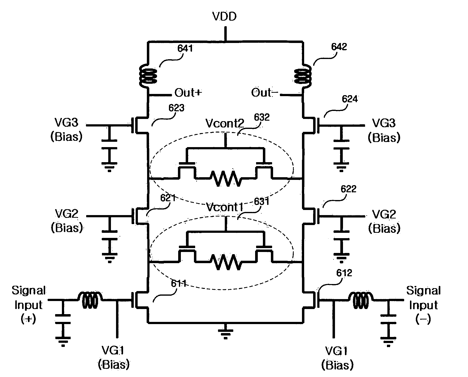
The present invention provides a variable gain amplifier with stable input / output matching characteristics. The amplifier includes a first cascode amplifier and a second cascode amplifier, which form a differential pair. A gain adjustment unit is connected to the drain of the first common source transistor and the source of the first common gate transistor, as well as the drain of the second common source transistor and the source of the second common gate transistor. The amplifier can have a stable input / output matching characteristic, which makes it easier to connect the amplifier to other components in a circuit.

Problems solved by technology

However, the variable gain amplifier has a small gain adjustment range and shows unstable input / output matching characteristics especially when being used as a high frequency circuit.
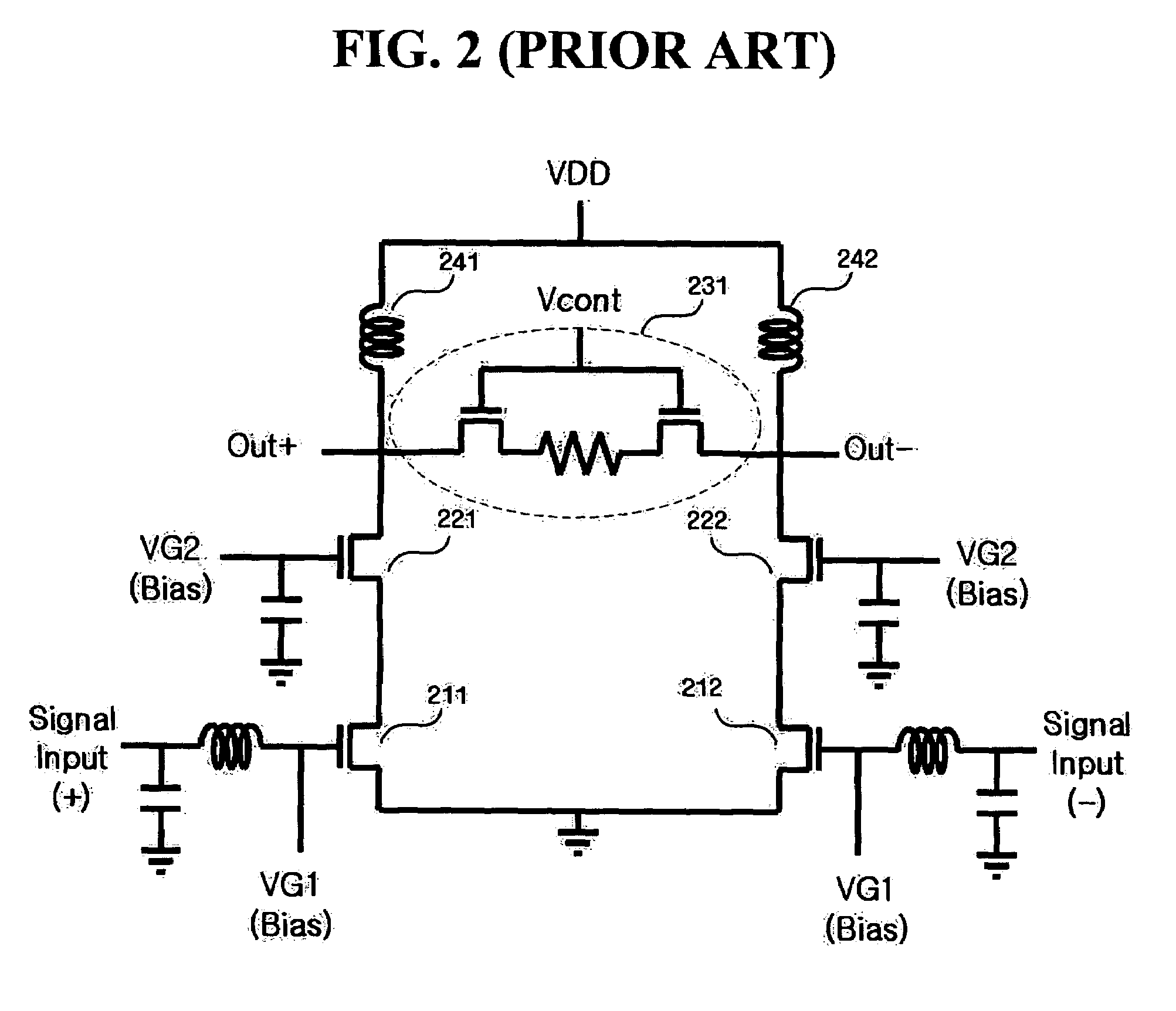
However, the conventional variable gain amplifier shown in FIG. 2 is undesirable in the low gain mode in terms of output matching characteristics because the output impedance of the conventional variable gain amplifier shown in FIG. 2 varies depending on whether the gain adjustment unit 231 is turned on or off.
A variable gain amplifier optimized for a high gain mode is highly likely to end up having poor input / output matching characteristics in a low gain mode, while a variable gain amplifier optimized for the low gain mode is highly likely to end up having poor input / output matching characteristics in the high gain mode.

Method used


Image

  • Variable gain amplifier
  • Variable gain amplifier
  • Variable gain amplifier

Examples


Embodiment Construction

[0044]Aspects of the present invention and methods of accomplishing the same may be understood more readily by reference to the following detailed description of exemplary embodiments and the accompanying drawings. The present invention may, however, be embodied in many different forms and should not be construed as being limited to the exemplary embodiments set forth herein. Rather, these exemplary embodiments are provided so that this disclosure will be thorough and complete and will fully convey the concept of the invention to those skilled in the art, and the present invention will only be defined by the appended claims.

[0045]The present invention will now be described more fully with reference to the accompanying drawings, in which exemplary embodiments of the invention are shown.

[0046]FIG. 4 is a circuit diagram of a variable gain amplifier according to an exemplary embodiment of the present invention.

[0047]Referring to FIG. 4, the variable gain amplifier has a differential ca...


PUM


Abstract

A variable gain amplifier is provided. The variable gain amplifier includes a first cascode amplifier which includes a first common source transistor and a first common gate transistor, a second cascode amplifier which forms a differential pair with the first cascode amplifier and includes a second common source transistor and a second common gate transistor, and a gain adjustment unit having a side connected to the drain of the first common source transistor and the source of the first common gate transistor and another side connected to the drain of the second common source transistor and the source of the second common gate transistor.

Description

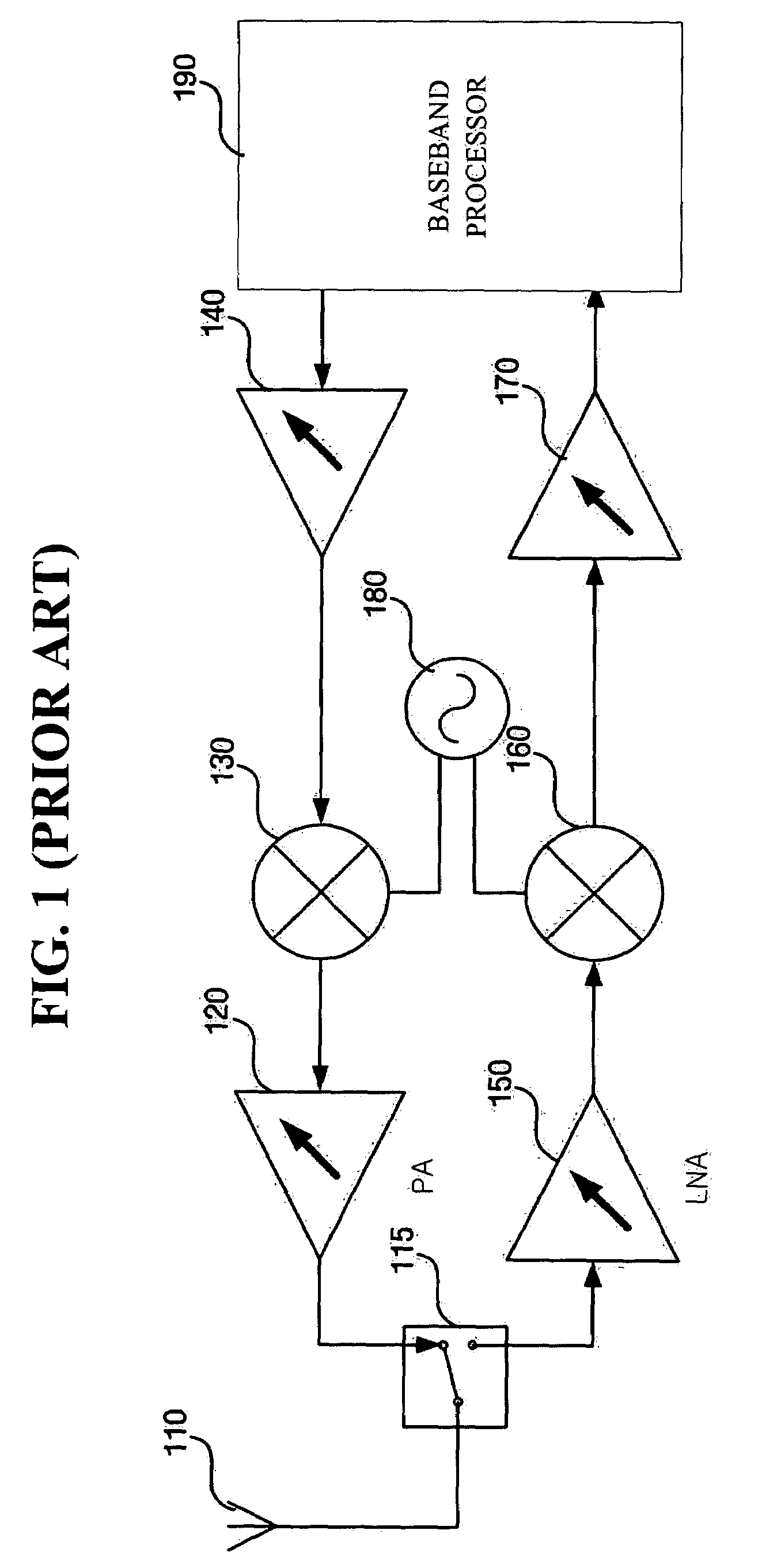
CROSS-REFERENCE TO RELATED APPLICATION[0001]This application claims priority from Korean Patent Application No. 10-2004-0078747 filed on Oct. 4, 2004 in the Korean Intellectual Property Office, the disclosure of which is incorporated herein by reference in its entirety.BACKGROUND OF THE INVENTION[0002]1. Field of the Invention[0003]The present invention relates to a variable gain amplifier, and more particularly, to a variable gain amplifier having stable input / output matching characteristics.[0004]2. Description of the Related Art[0005]In transmitting a signal using a wireless communication apparatus, in order to maintain the power of a signal output via an antenna constant, or to provide a signal received via the antenna with an appropriate gain according to the intensity of the received signal, the wireless communication apparatus needs a variable gain amplifier.[0006]FIG. 1 is a circuit diagram of an exemplary wireless communication apparatus including a variable gain amplifier....

Claims


Application Information

Patent Timeline
Patent Type & Authority Patents(United States)
IPC IPC(8): H03F3/45H03G3/00
CPCH03F3/45188H03G1/0088H03F2200/294H03F2200/372H03F2203/45318H03F2203/45396H03F2203/45544H03F2203/45548H03F2203/45554H03F2203/45638H03F2203/45376H03G3/10H03F3/45
Inventor LEE, JEONG-HO
Owner SAMSUNG ELECTRONICS CO LTD
Learn More