
Method for fabricating semiconductor packages

a technology for semiconductor packages and semiconductor components, applied in semiconductor devices, semiconductor/solid-state device details, electrical apparatus, etc., can solve the problems of significant difficulty in fabrication of bga semiconductor packages, waste of substrate utilization, and increased overall cost by about 15 to 20%, and achieves easy separation, poor adhesion, and convenient fabrication

Active Publication Date: 2008-03-25
SILICONWARE PRECISION IND CO LTD
View PDF8 Cites 8 Cited by
  • Summary
  • Abstract
  • Description
  • Claims
  • Application Information

AI Technical Summary

Benefits of technology

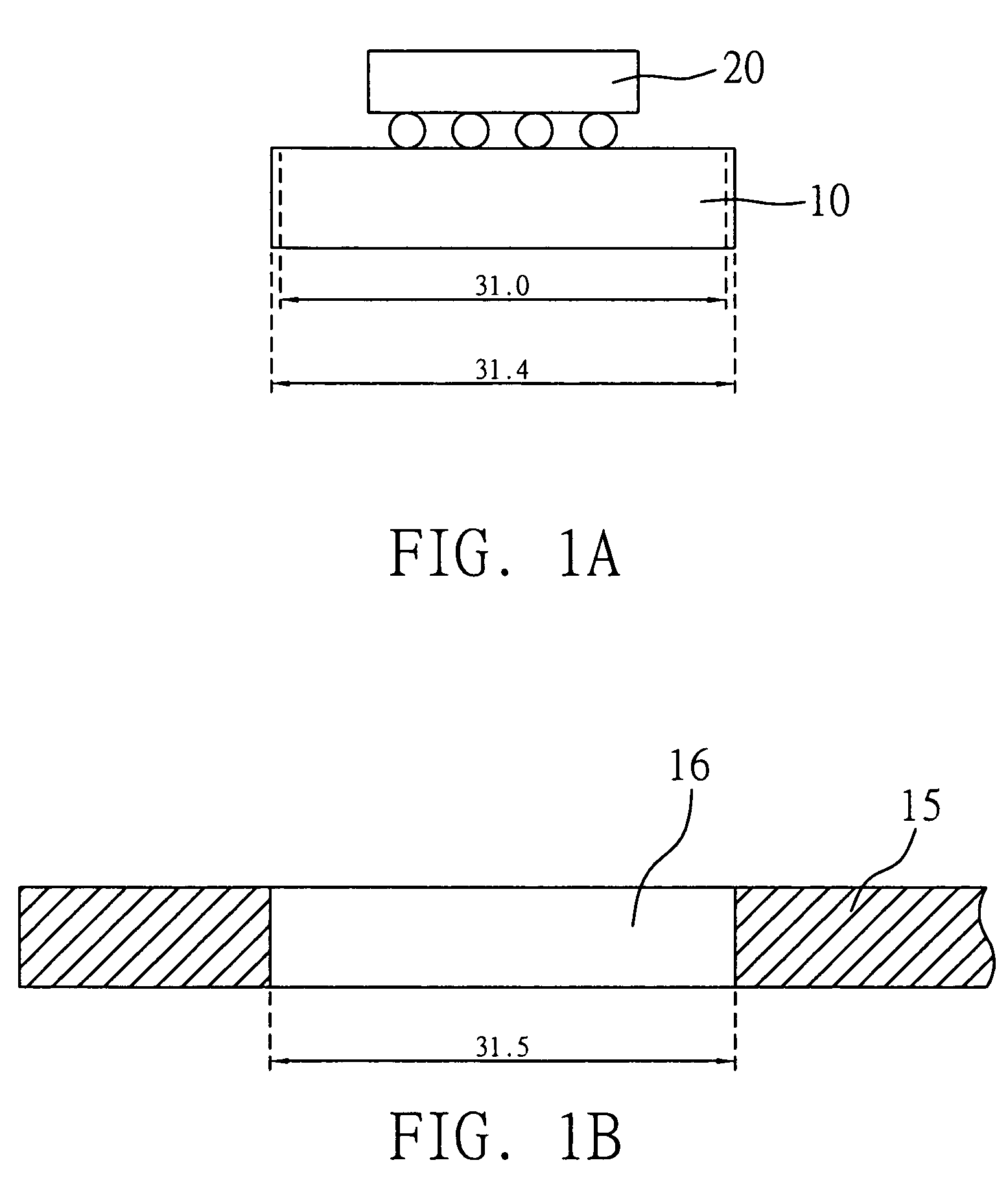
[0008]In light of the above drawbacks in the conventional technology, a primary objective of the present invention is to provide a method for fabricating semiconductor packages, which can reduce the substrate cost.
[0009]Another objective of the present invention is to provide a method for fabricating semiconductor packages, which does not require an increase in length and width of a substrate.
[0010]A further objective of the present invention is to provide a method for fabricating semiconductor packages, which can prevent flashes of an encapsulant without increasing the size of a substrate.
[0015]The metal carrier can be made of a copper (Cu) material, and a surface thereof is plated with a metal layer that is poorly adhesive to the encapsulant. The metal layer can be made of a metal material such as gold (Au), nickel (Ni), or chromium (Cr), etc. By virtue of the poor adhesion between the plated metal layer and the encapsulant, the package units can be easily separated from the metal carrier and thus provide convenience in fabrication.
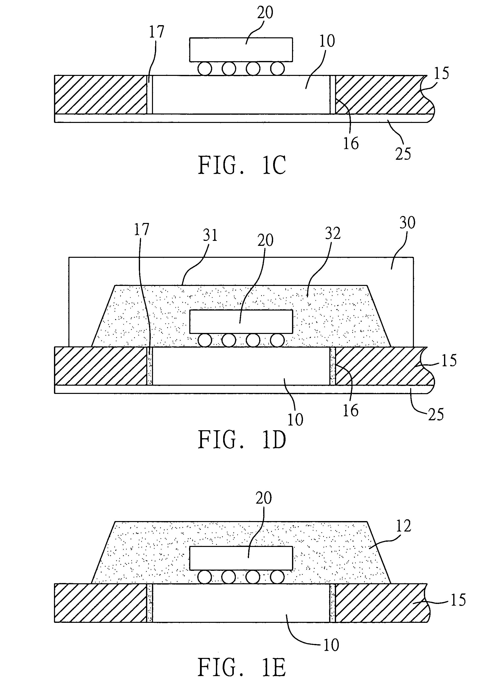
[0016]Therefore, according to the foregoing arrangement in the present invention, the substrate can have similar or substantially equal length and width to the predetermined length and width of the semiconductor package respectively, without having to over size the substrate. Moreover, the gaps between the substrates and the carrier are sealed, and the area on the carrier covered by the encapsulant is larger than the size of the opening of the carrier by using a mold cavity having coverage larger in length and width than the opening, such that resin flashes during the molding process and difficulty in mold releasing can be prevented. As a result, unnecessary increase in size and material of the substrate is avoided, thereby overcoming the drawbacks in the conventional technology.

Problems solved by technology

The increase of substrate size not only causes a waste of substrate utilization but also makes the overall costs increased by about 15 to 20%.
The foregoing drawback leads to significant difficulty in fabrication of the BGA semiconductor package.
The molding process for forming the encapsulant 73 is an essential step in the package fabrication, however it makes the size and material cost of the substrate 70 increased, thereby not advantageous for mass production.

Method used


Image

  • Method for fabricating semiconductor packages
  • Method for fabricating semiconductor packages
  • Method for fabricating semiconductor packages

Examples


first preferred embodiment

[0029]FIGS. 1A to 1H show steps of a method for fabricating semiconductor packages according to a first preferred embodiment of the present invention. Referring to FIG. 1A, firstly, a plurality of build-up substrates 10 (only one is shown) each carrying at least one chip 20 thereon are prepared. Each of the substrates 10 has slightly larger length and width than the predetermined length and width of a final semiconductor package 1 (shown in FIG. 1H) respectively. In this embodiment, the predetermined dimensions of the semiconductor package 1 after singulation are 31 mm×31 mm in length and width, such that the length and width of the substrate 10 are sized 31.4 mm×31.4 mm. Then, referring to FIG. 1B, a substrate carrier 15 having a plurality of openings 16 (only one is shown) is prepared, wherein each of the openings 16 is larger in length and width than each of the substrates 10, such that the substrates 10 carrying the chips 20 thereon can be embedded and positioned in the correspo...

second preferred embodiment

[0035]Apart from the above first embodiment in which the substrate 10 has slightly larger length and width than the predetermined length and width of the semiconductor package 1, the substrate 10 can be sized slightly smaller in length and width than the semiconductor package 1 to further reduce the material used for the substrate 10 according to a second preferred embodiment shown in FIGS. 4A to 4H wherein similarly, the predetermined size of the semiconductor package 1 after singulation is 31 mm×31 mm in length and width.

[0036]Referring to FIG. 4A, firstly, a plurality of build-up substrates 10 (only one is shown) each carrying at least one chip 20 thereon are prepared. Each of the substrates 10 has its length and width sized 30.8 mm×30.8 mm and slightly smaller than the predetermined length and width of the semiconductor package 1 (31 mm×31 mm as shown in FIG. 4H). Referring to FIG. 4B, a carrier 15 having a plurality of openings 16 (only one is shown) is prepared. Each of the op...

third preferred embodiment

[0040]Apart from the carrier 15 made of an organic insulating material such as FR4, FR5, BT, and so on, a metal carrier having a metal layer plated on a surface thereof can be used in the present invention according to a third preferred embodiment shown in FIGS. 5A to 5I. The metal layer is made of a material poorly adhesive to the encapsulant 32. In the third embodiment, the predetermined size of the semiconductor package 1, the size of the substrate 10, and the size of an opening 46 of a carrier 45 are all same as those described in the foregoing embodiments. Only the material used for the carrier 45 and some of the fabrication processes in the third embodiment are different from those in the foregoing embodiments.

[0041]Referring to FIG. 5A, firstly, a plurality of build-up substrates 10 (only one is shown) each carrying at least one chip 20 thereon are prepared. The length and width of each of the substrates 10 are 31.4 mm×31.4 mm, and the predetermined length and width of the se...


PUM


Abstract

A method for fabricating semiconductor packages is proposed. A plurality of substrates each having a chip thereon are prepared. Each substrate has similar length and width to the predetermined length and width of the semiconductor package. A carrier having a plurality of openings is prepared. Each opening is larger in length and width than the substrate. The substrates are positioned in the corresponding openings, and gaps between the substrates and the carrier are sealed. A molding process is performed to form an encapsulant over each opening to encapsulate the chip. An area on the carrier covered by the encapsulant is larger in length and width than the opening. After performing a mold-releasing process, a plurality of the semiconductor packages are formed by a singulation process to cut along substantially edges of each substrate according to the predetermined size of the semiconductor package. A waste of substrate material is avoided.

Description

FIELD OF THE INVENTION[0001]The present invention relates to methods for fabricating semiconductor packages, and more particularly, to a method using a substrate carrier to fabricate ball grid array (BGA) semiconductor packages.BACKGROUND OF THE INVENTION[0002]Flip-chip ball grid array (FCBGA) semiconductor package relates to a combination of flip chip and ball grid array, which allows an active surface of at least one chip mounted therein to be electrically connected to a surface of a substrate via a plurality of solder bumps, and a plurality of solder balls to be implanted on another surface of the substrate, wherein the solder balls serve as input / output (I / O) connections for the semiconductor package. This semiconductor package yields significant advantages to effectively decrease the package size, reduce resistance and improve electrical performances to prevent decay of signals during transmission without using conventional bonding wires. Therefore, the FCBGA semiconductor pack...

Claims


Application Information

Patent Timeline
Patent Type & Authority Patents(United States)
IPC IPC(8): H01L21/50H01L21/44H01L21/48H01L21/56H01L21/68H01L23/31
CPCH01L21/565H01L21/568H01L23/3128H01L24/48H01L2224/16225H01L2224/48227H01L2224/73204H01L2224/73253H01L2924/15311H01L2224/16227H01L2924/181H01L2924/00014H01L2924/00012H01L2224/45099H01L2224/45015H01L2924/207
Inventor LIN, YING-RENTSAI, HO-YIHUANG, CHIEN-PINGHSIAO, CHENG-HSU
Owner SILICONWARE PRECISION IND CO LTD
Learn More