Silicon carbide diode voltage limiter

a silicon carbide diode and voltage limiter technology, applied in the direction of emergency protective circuit arrangements, emergency protective arrangements for limiting excess voltage/current, emergency protective arrangements, etc., can solve the problems of limiting the time to failure of the switch, damaging the contacts, and deleterious voltage spikes

Inactive Publication Date: 2008-03-04
ROCKETDYNE
View PDF3 Cites 12 Cited by
  • Summary
  • Abstract
  • Description
  • Claims
  • Application Information

AI Technical Summary

Benefits of technology

[0006]The present invention provides a voltage excursion control system for limiting transient voltage peaks in electrical circuits otherwise occurring across selected components therein in response to changing conditions in such circuits with the system having a plurality of silicon carbide diode dice each having an anode and a cathode region therein and each positioned in a spatial succession thereof. Each such die is interconnected by an electrically conductive metal bond with each neighbor thereof in the succession such that each cathode region of each die face toward a common end of the succession. First and second electrically conductive electrodes are each electrically interconnected by an electrically conductive metal bond with a corresponding one of the dice at opposite ends of the succession. The electrode interconnected to an anode region of a die is so interconnected by one of a pair of extensions provided in that electrode with a gap between them in which the succession and the remaining electrode are positioned. An antiparallel diode die has a cathode region therein electrically interconnected by an electrically conductive metal bond with that remaining one of the pair of extensions and has an anode region therein electrically interconnected by an electrically conductive metal bond with the remaining one of the first and second electrodes

Problems solved by technology

Such voltage spikes are deleterious to the switch because the large voltage causes an electrical discharge across the gap between the separating switch contacts as the switch is being opened leading to damaging those contacts and so limiting the time to failure of that switch.
Though the lower plot shows the circuit current decreases to zero following this switching event, there is still substantial current in the circuit at the time of occurrence of the voltage spike to thereby result in a corresponding electrical power spike.
Without a snubber arrangement of some kind across switch 4, this transient voltage peak and the associated arc discharge will damage, and so reduce the operational duration of, the switch contacts.
These configurations tended to be relatively large.
While these devices are much smaller than the filter arrangement, the response and power rating of these devices make their suitability in substantial power handling circuits limited.

Method used


Image

  • Silicon carbide diode voltage limiter
  • Silicon carbide diode voltage limiter
  • Silicon carbide diode voltage limiter

Examples


Embodiment Construction

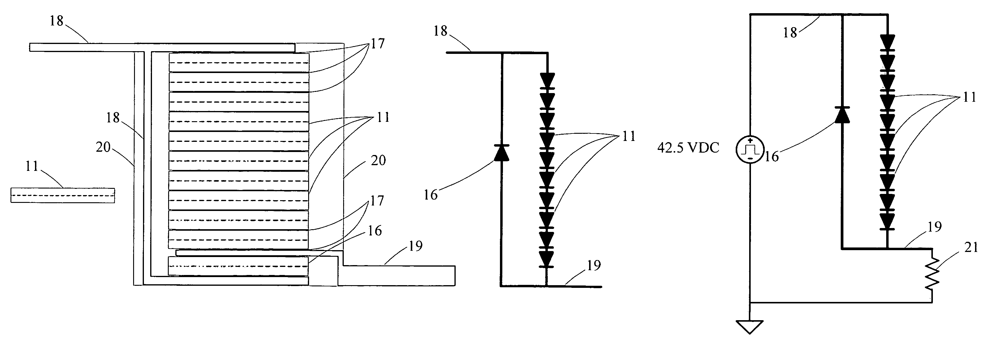
[0013]A basis for a more suitable voltage excursion control circuit is provided by using a high voltage silicon carbide (SiC) p-i-n diode, a p-n junction diode having an intrinsic, or lightly doped region, positioned between the p and n regions in the diode. Such a diode for a snubber arrangement must configured to be capable of carrying large electrical currents therethrough to accommodate the large current transients that will ensue in limiting voltage peaks during the control switchings that occur in controlling power flows in large electrical power flow circuits. In addition, these large electrical currents through that diode are desired to be associated with substantial forward voltage drops across the diodes to allow relatively few such diodes being connected in series to set the snubber breakover voltage suited for the voltage levels encountered during steady state operations of the power circuit having its switch being protected by the provision of the snubber arrangement. A...


PUM


Abstract

A voltage excursion control system for limiting transient voltage peaks in electrical circuits otherwise occurring across selected components therein in response to changing conditions in such circuits has a plurality of silicon carbide diode dice series-interconnected in a succession such that each cathode region of each die face toward a common end of the succession. First and second electrically conductive electrodes are each electrically interconnected with a corresponding one of the dice at opposite ends of the succession.

Description

BACKGROUND OF THE INVENTION[0001]The present invention relates to limiting voltage excursions in electrical circuits including suppressing transient voltage peaks, and, more particularly, to suppressing them quickly.[0002]A “snubber” arrangement is used in electrical circuits where there is the possibility of large voltage peaks, or voltage “spikes”, occurring in those circuits, often immediately following a switch being opened in the circuit because of inductance in that circuit causing a transient voltage peak, i.e. an inductive “kick”. Such voltage spikes are deleterious to the switch because the large voltage causes an electrical discharge across the gap between the separating switch contacts as the switch is being opened leading to damaging those contacts and so limiting the time to failure of that switch.[0003]As an example, FIG. 1A shows a schematic diagram of a representative circuit, 1, in which power flows occur subject to being switched on and off. Circuit 1 contains an i...

Claims


Application Information

Patent Timeline
Patent Type & Authority Patents(United States)
IPC IPC(8): H02H3/22H01L31/0312
CPCH01L23/62H01L25/074H02H9/043H01L24/29H01L24/32H01L2224/29144H01L2224/32145H01L2224/32245H01L2924/01032H01L2924/01079H01L2924/01322
Inventor HERTEL, THOMAS A.TAN, DANIEL
Owner ROCKETDYNE
Why Eureka
Try Eureka