Electromagnetic wave frequency filter
a technology filter body, which is applied in the direction of waveguides, waveguide type devices, instruments, etc., can solve the problems of difficult design and manufacture of electromagnetic wave frequency filter, inefficient drop efficiency, etc., and achieve the effect of reducing energy consumption and speeding up switching speed
- Summary
- Abstract
- Description
- Claims
- Application Information
AI Technical Summary
Benefits of technology
Problems solved by technology
Method used
Image
Examples
first embodiment
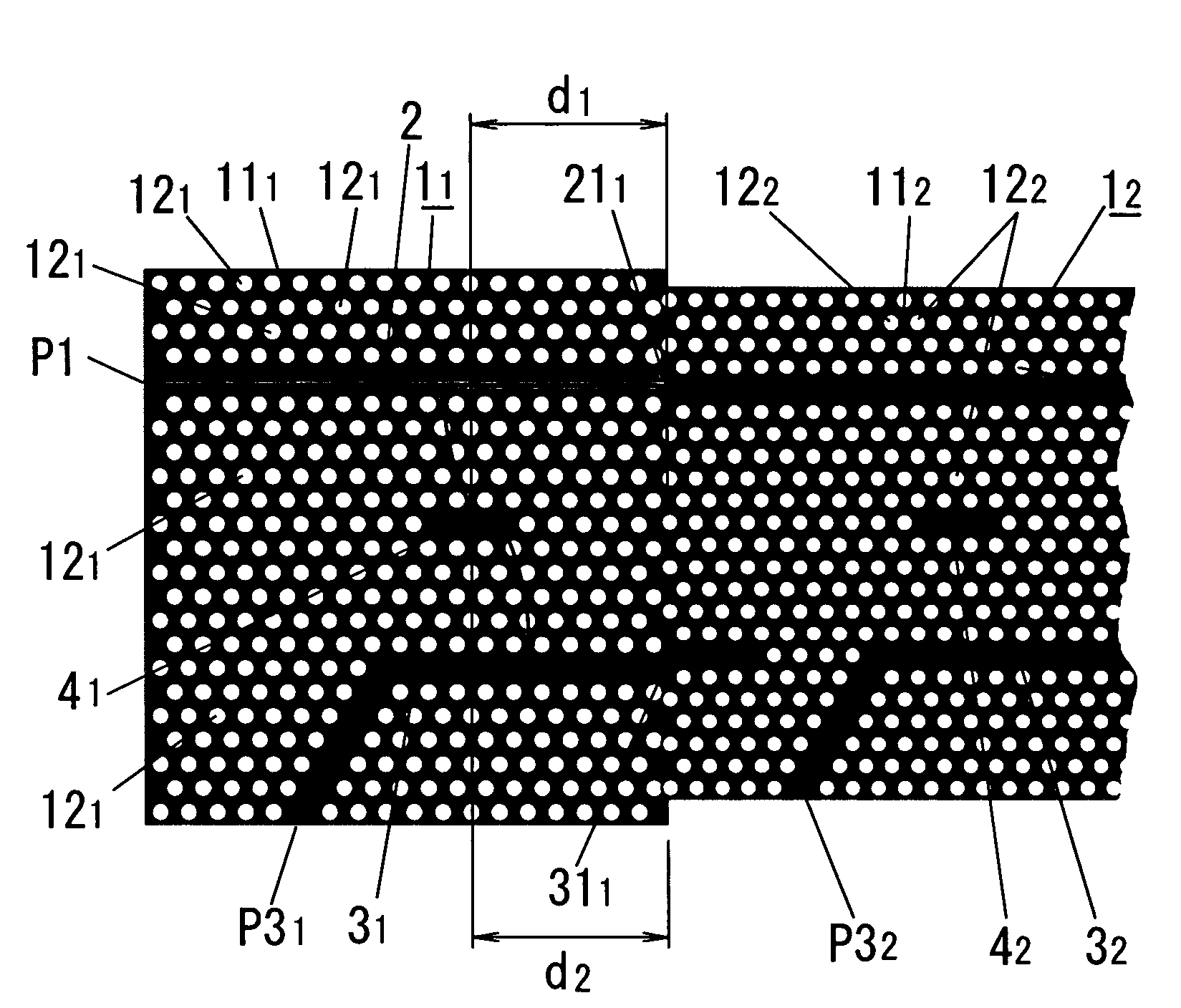
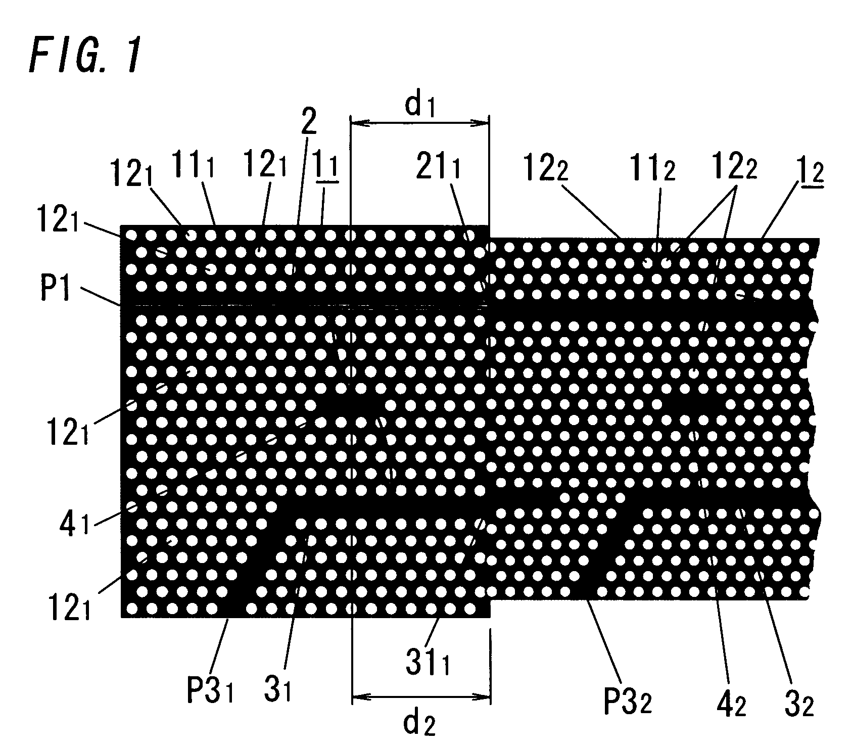
[0052]As shown in FIG. 1, an electromagnetic wave frequency filter of this embodiment has an in-plane heterostructure in which a plurality of two-dimensional photonic crystals 11, 12, . . . each having a refractive-index periodic structure whoso period is different from the others are placed side by side in one direction (horizontal direction of FIG. 1) in a two-dimensional plane (in FIG. 1, only two two-dimensional photonic crystals 11, 12 are shown). The electromagnetic wave frequency filter has an input waveguide 2, which are formed by creating a linear defect in the refractive-index periodic structures of all the two-dimensional photonic crystals 11, 12, . . . along the entire length of the two-dimensional photonic crystals in an arranging direction of the two-dimensional photonic crystals 11, 12, . . . . The electromagnetic wave frequency filter also has output waveguides 31, 32, . . . , each of which is formed by creating a linear defect in the refractive-index periodic struct...
second embodiment
[0067]In the electromagnetic wave frequency filter of the first embodiment, the resonators 41, 42, . . . was disposed so that all resonators 41, 42, . . . were arranged on a straight line, and the periods of the refractive-index periodic structure in each pair of two-dimensional photonic crystals 1n, 1m (n=1, 2, . . . , m=n+1) adjacent to each other in the arranging direction of these two-dimensional photonic crystals 11, 12, . . . were different from each other. So, the input waveguide 2 had the axis misalignment (the misalignment of the optical axis) between the portion of the input waveguide formed in the former two-dimensional photonic crystal 1n (in FIG. 1, in the two-dimensional photonic crystal 11) and the portion of the input waveguide formed in the latter two-dimensional photonic crystal 1m (in FIG. 1, in the two-dimensional photonic crystal 12). As a result, reflection losses resulting from the axis misalignment of the input waveguide 2 were generated to the electromagneti...
third embodiment
[0071]In the electromagnetic wave frequency filter of the second embodiment, because the input waveguide 2 extended smoothly and continuously near the boundary of each pair of two-dimensional photonic crystals 1n, 1m, the reflection losses resulting from the axis misalignment of the input waveguide 2 with respect to the electromagnetic waves of the frequencies different from the resonant frequency of the resonator 4n can be reduced, whereby the drop efficiency of the posterior drop port P32, . . . can be increased, as compared with the first embodiment. However, even in the electromagnetic wave frequency filter of the second embodiment, the reflection losses resulting from the axis misalignment of the input waveguide 2 are generated, so that the drop efficiency of each drop port P31, P32, . . . becomes different from each other. So, it is desired to further increase the drop efficiency (wavelength selection efficiency) of the posterior drop port P32, . . . .
[0072]The electromagnetic...
PUM
| Property | Measurement | Unit |
|---|---|---|
| thickness | aaaaa | aaaaa |
| refractive index | aaaaa | aaaaa |
| refractive index | aaaaa | aaaaa |
Abstract
Description
Claims
Application Information
 - R&D
- Intellectual Property
- Life Sciences
- Materials
- Tech Scout
- Unparalleled Data Quality
- Higher Quality Content
- 60% Fewer Hallucinations
Browse by: Latest US Patents, China's latest patents, Technical Efficacy Thesaurus, Application Domain, Technology Topic, Popular Technical Reports.
© 2025 PatSnap. All rights reserved.Legal|Privacy policy|Modern Slavery Act Transparency Statement|Sitemap|About US| Contact US: help@patsnap.com


