
Liquid crystal display wiring pattern having gate lines and storage electrode lines

a technology of gate lines and liquid crystal display, which is applied in non-linear optics, instruments, optics, etc., can solve the problems of increasing manufacturing costs and light leakage still remaining, and achieve the effects of improving the opening ratio, improving the contrast ratio, and reducing the disclination degree of liquid crystal material

Inactive Publication Date: 2008-01-08
SAMSUNG DISPLAY CO LTD
View PDF22 Cites 6 Cited by
  • Summary
  • Abstract
  • Description
  • Claims
  • Application Information

AI Technical Summary

Benefits of technology

[0014]It is another object of the present invention to provide liquid crystal display devices having improved opening ratios and methods of forming same.
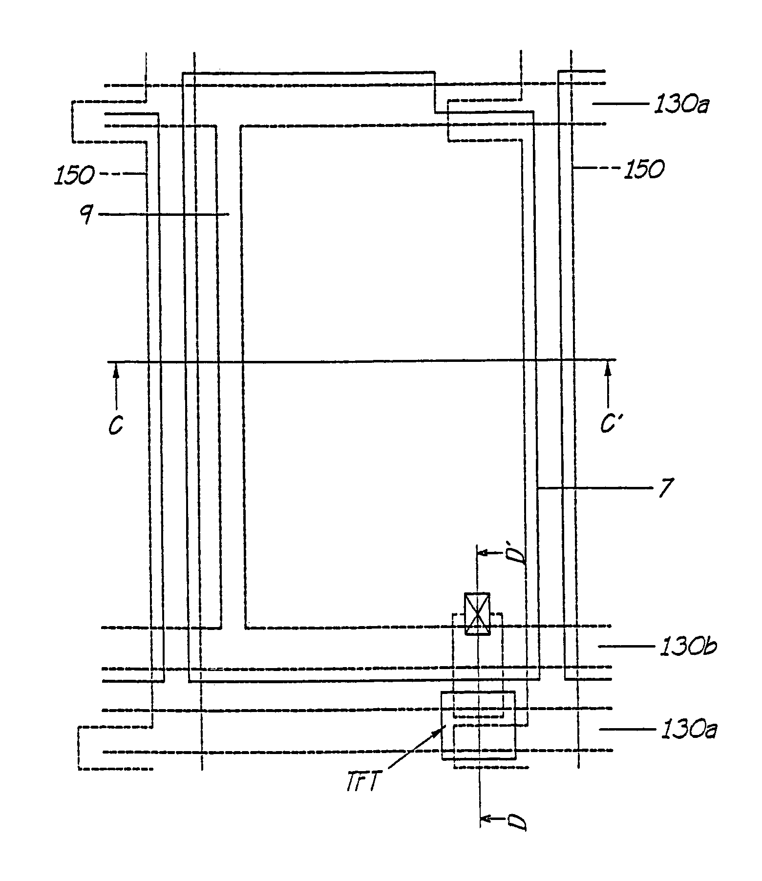
[0022]Thus, the present invention provides for liquid crystal display devices having improved contrast ratios by incorporating light blocking lines therein. The light blocking lines are also patterned so that any step height in the display's pixel electrodes is maintained at a low level so that the degree of disclination in the liquid crystal material is reduced. This is achieved by patterning the light blocking lines so that they do not overlap the display's data lines. In addition, the light blocking lines are preferably positioned on only one side of the data lines so that improved opening ratios can be achieved. The parasitic loading capacitance between the data lines and pixel electrodes can also be improved by patterning the light blocking lines below the data lines, using the same level of metallization as used to form the gate lines.

Problems solved by technology

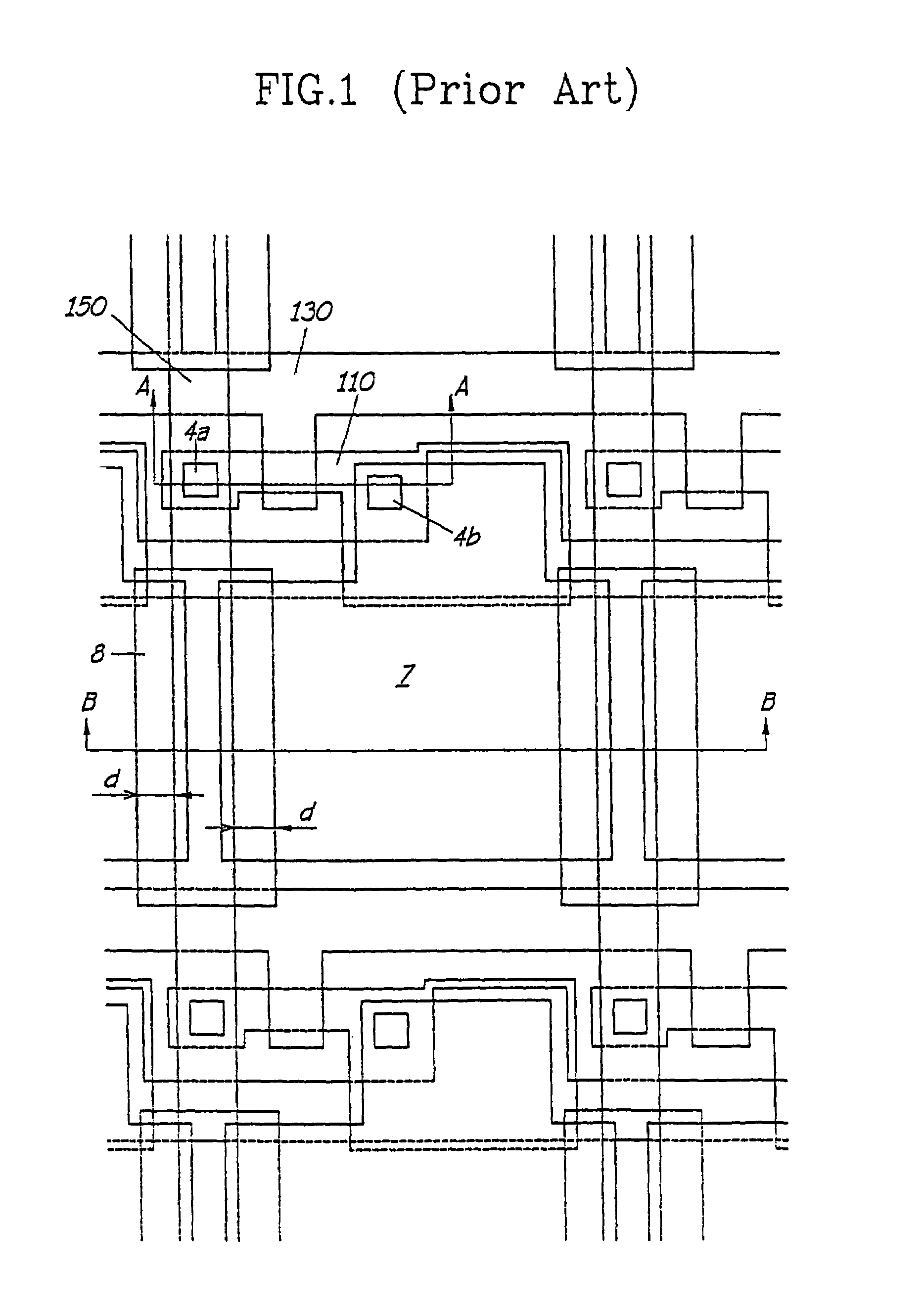
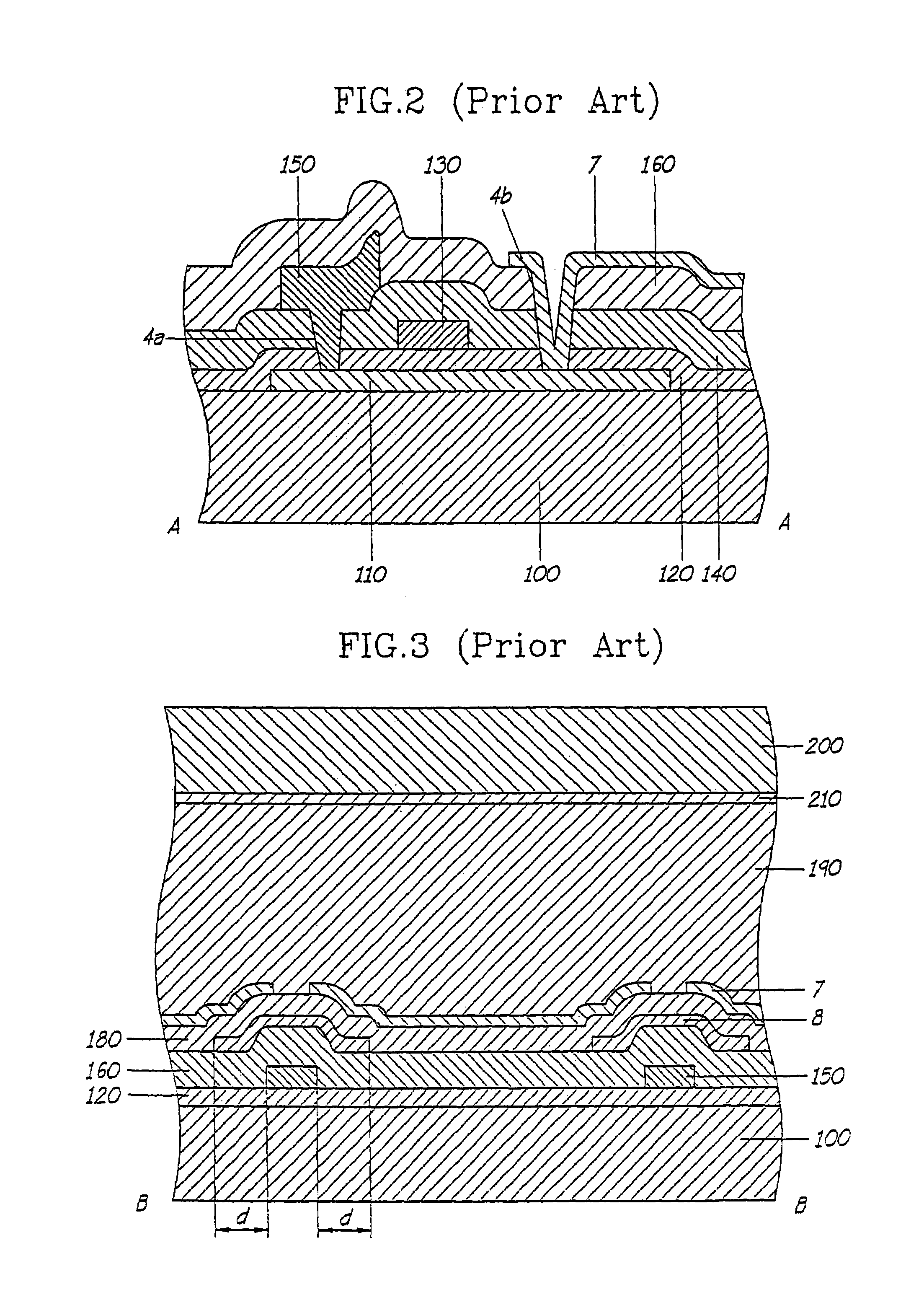
However, some light leakage still remains due to the considerable step of the data line 150.
Moreover, the fabrication of this structure where the light blocking film 8 is formed on the data line 150 increases manufacturing cost since it requires additional processes such as metal deposition and etching.

Method used


Image

  • Liquid crystal display wiring pattern having gate lines and storage electrode lines
  • Liquid crystal display wiring pattern having gate lines and storage electrode lines
  • Liquid crystal display wiring pattern having gate lines and storage electrode lines

Examples


Embodiment Construction

[0033]The present invention will now be described more fully hereinafter with reference to the accompanying drawings, in which preferred embodiments of the invention are shown. This invention may, however, be embodied in different forms and should not be construed as limited to the embodiments set forth herein. Rather, these embodiments are provided so that this disclosure will be thorough and complete, and will fully convey the scope of the invention to those skilled in the art. Like numbers refer to like elements throughout.

[0034]Referring to FIGS. 4 and 10, layout and electrical schematic diagrams of an active matrix liquid crystal display device according to the present invention will now be described. In particular, an active matrix liquid crystal display device is provided which comprises a two-dimensional array of thin-film transistor (TFT) liquid crystal display cells arranged as a plurality of columns of display cells and a plurality of rows of display cells.

[0035]As illust...


PUM

PropertyMeasurementUnit
thicknessaaaaaaaaaa
thicknessaaaaaaaaaa
thicknessaaaaaaaaaa

Abstract

A liquid crystal display comprises a first wiring pattern formed on a substrate. The first wiring pattern comprises a gate line, a gate electrode and a storage electrode line. A first insulating layer is formed on the first wiring pattern. A semiconductor pattern is formed on the first insulating layer. A second wiring pattern is formed on the semiconductor pattern and the first insulating layer. The second wiring pattern comprises a data line, a source electrode and a drain electrode. The drain electrode at least partially overlaps the storage electrode line. A second insulating layer is formed on the second wiring pattern. The second insulating layer has an opening exposing the drain electrode. A pixel electrode is formed on the second insulating layer and connected to the drain electrode via the opening. The storage electrode line has a branch extending parallel to the data line. The pixel electrode overlaps the gate line of the previous row.

Description

CROSS REFERENCE[0001]This application is a continuation application of Applicant's U.S. patent application Ser. No. 10 / 427,139 filed on May 2, 2003 now U.S. Pat. No. 6,791,630; which is a divisional application of U.S. patent application Ser. No. 09 / 829,818 filed on Apr. 10, 2001, issued as U.S. Pat. No. 6,580,473; which is a divisional application of U.S. patent application Ser. No. 08 / 884,607 filed on Jun. 30, 1997, issued as U.S. Pat. No. 6,262,784; which is a continuation-in-part application of U.S. patent application Ser. No. 08 / 602,104 filed on Feb. 23, 1996, issued as U.S. Pat. No. 5,696,566; which is a divisional application of application Ser. No. 08 / 070,717 filed on Jun. 1, 1993, issued as U.S. Pat. No. 5,517,341, each of which is herein specifically incorporated by reference in their entireties.FIELD OF THE INVENTION[0002]The present invention relates to display devices and methods of forming display devices, and more particularly to liquid crystal display devices and met...

Claims


Application Information

Patent Timeline
Patent Type & Authority Patents(United States)
IPC IPC(8): G02F1/1343G02F1/13G02F1/136G02F1/1335G02F1/1362
CPCG02F1/1309G02F1/136213G02F1/136227G02F1/136286G02F1/133512G02F2001/136263G02F1/136263G02F1/136G02F1/1343
Inventor KIM, DONG-GYU
Owner SAMSUNG DISPLAY CO LTD
Learn More