
Compound semiconductor element based on Group III element nitride

a technology of nitride and compound semiconductors, which is applied in the direction of semiconductor devices, basic electric elements, electrical equipment, etc., can solve the problems that metal nitride having such a thickness has never been provided, and achieve the effects of improving crystallinity, good crystallinity, and good crystallinity

Inactive Publication Date: 2007-12-25
TOYODA GOSEI CO LTD
View PDF23 Cites 19 Cited by
  • Summary
  • Abstract
  • Description
  • Claims
  • Application Information

AI Technical Summary

Benefits of technology

[0013]In the semiconductor device configured as described above according to the invention, a Group III nitride compound semiconductor layer is formed on a metal nitride layer of (Ti1−xAx)N. This metal nitride layer becomes smaller in lattice misfit with the Group III nitride compound semiconductor layer formed on this metal nitride layer than a metal nitride layer of two elements such as TiN. Accordingly, the crystallinity of the Group III nitride compound semiconductor layer can be improved.
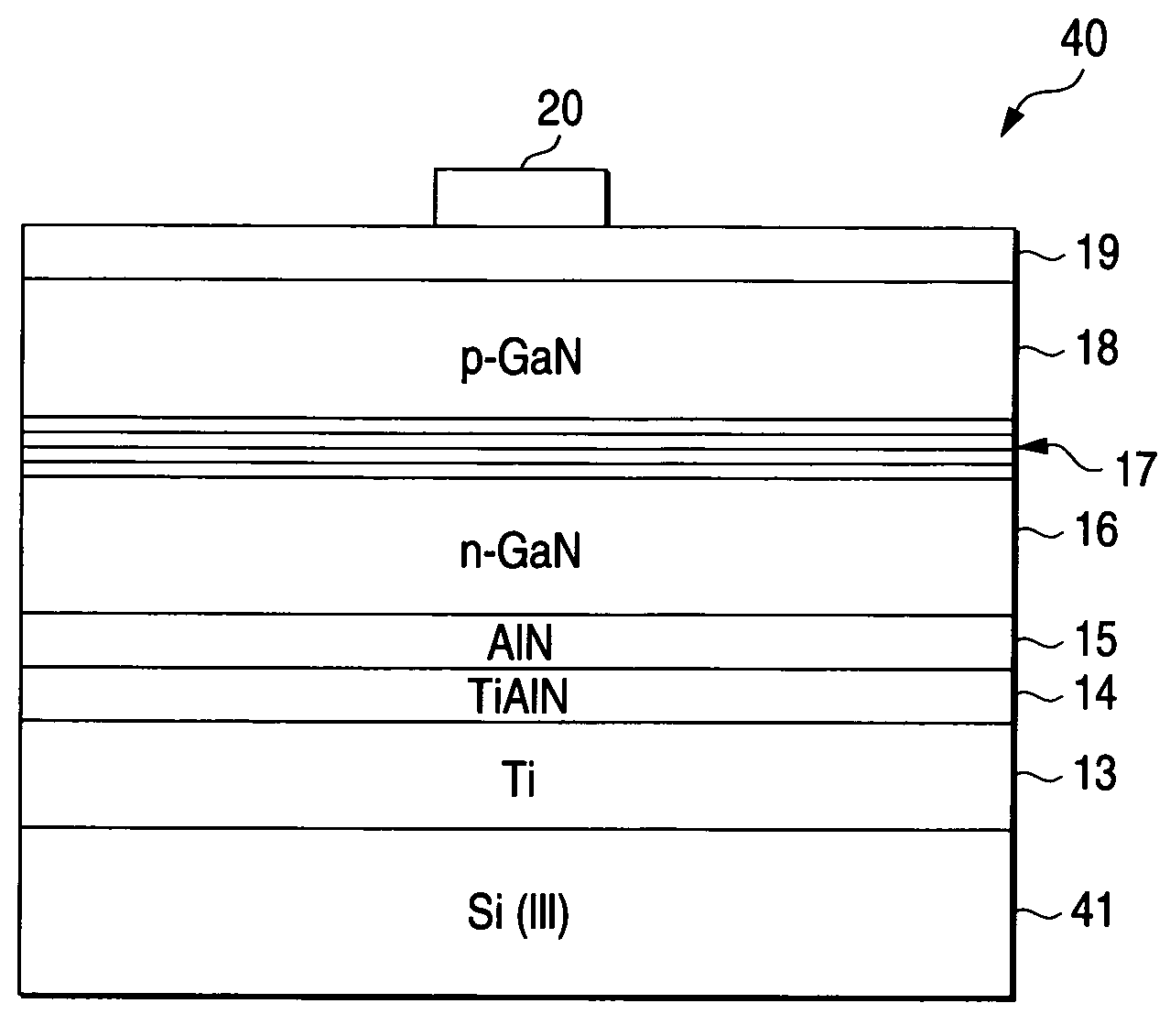
[0014]The metal nitride layer of (Ti1−xAx)N can be formed with good crystallinity on a substrate such as sapphire. Moreover, the metal nitride layer can be formed with good crystallinity on a titanium layer because the metal nitride layer contains Ti as a component, while the titanium layer can be formed with good crystallinity on a substrate such as sapphire. Moreover, the metal nitride layer can be made thin because the substrate having a thickness required for sustaining a function of the device can be obtained. Accordingly, the metal nitride layer can be formed easily and inexpensively. When a general-purpose material such as sapphire is used as the substrate, the device can be produced inexpensively as a whole.

Problems solved by technology

As a result, it has been found that there is fear that difference in lattice constant between TiN and a Group III nitride compound semiconductor may have influence on the crystallinity of the Group III nitride compound semiconductor.
Metal nitride having such a thickness has been never provided as a raw material of an industrial product used for producing a semiconductor.

Method used


Image

  • Compound semiconductor element based on Group III element nitride
  • Compound semiconductor element based on Group III element nitride
  • Compound semiconductor element based on Group III element nitride

Examples


first embodiment

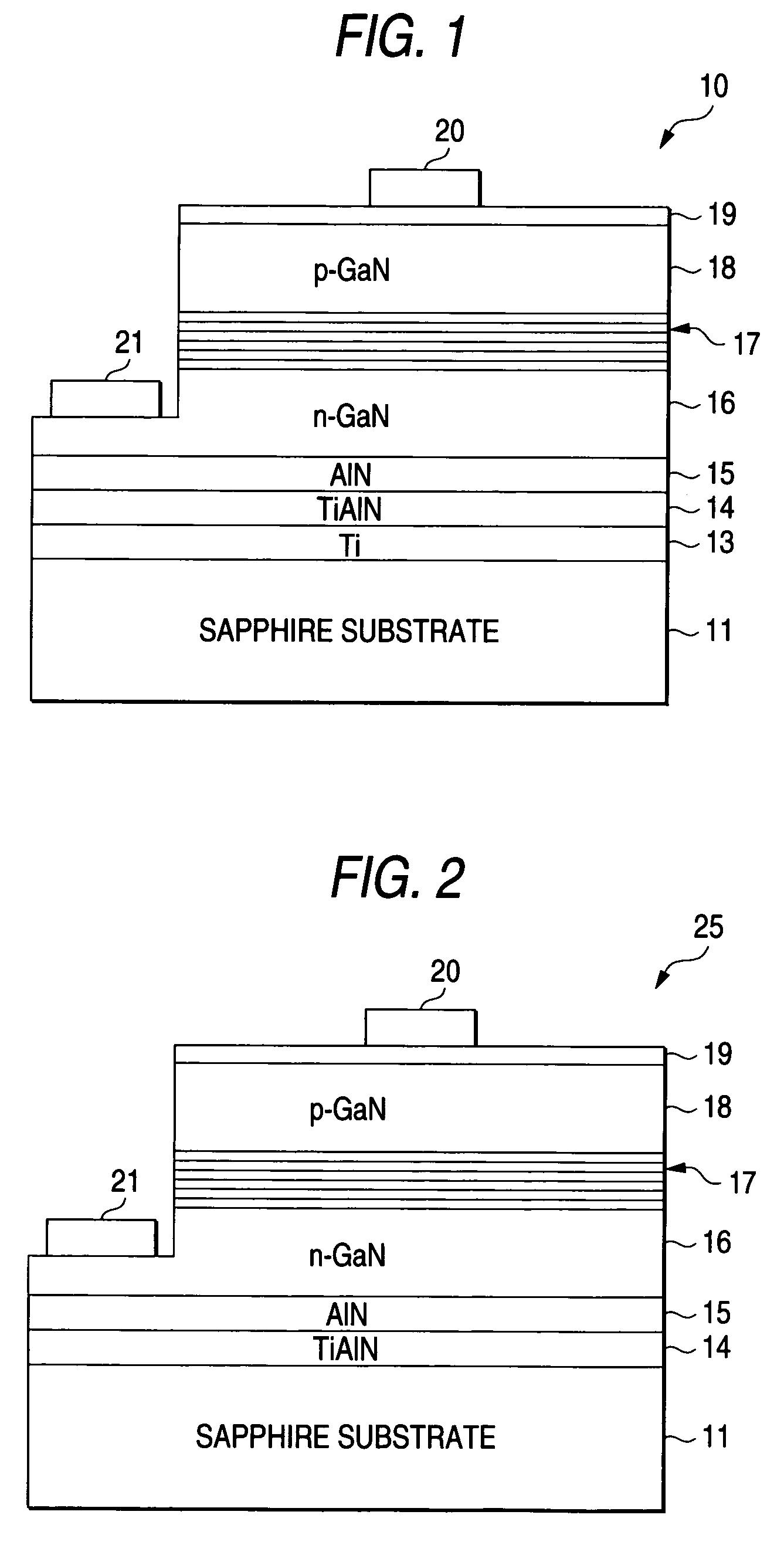
[0045]This embodiment shows a light-emitting diode 10. FIG. 1 shows the configuration of the light-emitting diode 10.

[0046]Specifications of respective layers are as follows.

[0047]

LayerComposition: Dopantp-type layer 18p-GaN: MgLayer 17 containing acontains a layer of InGaNlight-emitting layern-type layer 16n-GaN: SiBuffer layer 15AlNMetal nitride layer 14Ti0.97Al0.03NTi layer 13TiSubstrate 11sapphire

[0048]The n-type layer 16 may be of a double-layered structure with an n− layer of a low electron density on the layer 17 containing a light-emitting layer side and an n+ layer of a high electron density on the buffer layer 15 side. The latter is called “n-type contact layer”.

[0049]The layer 17 containing a light-emitting layer is not limited to a superlattice structure. A single hetero type structure, a double hetero type structure, a homo-junction type structure, or the like, may be used as the structure of the light-emitting device. A single quantum well structure may be also used.

[0...

second embodiment

[0058]FIG. 2 shows a light-emitting diode 25 according to a second embodiment. Incidentally, parts the same as those in the first embodiment are referred to by numerals the same as those in the first embodiment and their description will be omitted. The light-emitting diode 25 according to this embodiment is configured so that the Ti layer 13 is omitted from the light-emitting diode shown in FIG. 1. The metal nitride layer 14 is formed directly on the sapphire substrate.

[0059]Also in the light-emitting diode 25 configured as described above, Group III nitride compound semiconductor layers 16 to 18 of excellent crystallinity can be obtained.

third embodiment

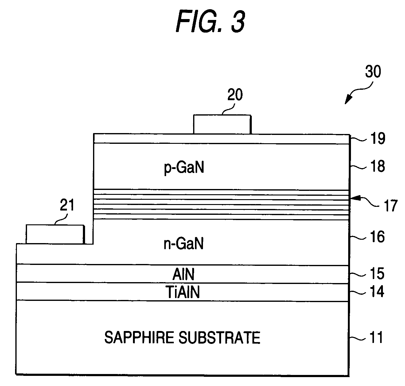
[0060]FIG. 3 shows a light-emitting diode 30 according to a third embodiment. Incidentally, parts the same as those in FIG. 2 are referred to by numerals the same as those in FIG. 2, and their description will be omitted. In the light-emitting diode 30 according to this embodiment, a configuration that an n-type electrode 21 is formed on the metal nitride layer 14 is applied to the light-emitting diode shown in FIG. 2. Because the metal nitride layer 14 has electrically conductive characteristic higher than that of the n-GaN layer 16, an electric current can be distributed into the Group III nitride compound semiconductor layers more uniformly as a whole. In addition, because the metal nitride layer 14 of TiAlN contains the same element (Al) as that of then-type electrode 21, contact resistance can be reduced as well as the adhesion between the two can be improved.


PUM

PropertyMeasurementUnit
thicknessaaaaaaaaaa
thicknessaaaaaaaaaa
lattice constantaaaaaaaaaa

Abstract

In the present invention, (Ti1−xAx)N [in which A is at least one kind of metal selected from the group consisting of Al, Ga, and In] is used as a metal nitride layer, so that a Group III nitride compound semiconductor layer is formed on the metal nitride layer. When a Ti layer is formed between the metal nitride layer having a sufficient thickness and a substrate and the titanium layer is removed, a Group III nitride compound semiconductor device using metal nitride as a substrate can be obtained.

Description

TECHNICAL FIELD[0001]The present invention relates to a Group III nitride compound semiconductor device.BACKGROUND ART[0002]Unexamined Japanese Patent Publication No. Hei-09-237938 has disclosed that a (111) face of metal nitride having a sodium chloride structure as an undercoat layer is used as a substrate for obtaining Group III nitride compound semiconductor layers of good crystallinity. That is, in this official gazette, metal nitride having a sodium chloride structure is used as a substrate and Group III nitride compound semiconductor layers are grown on the (111) face of the metal nitride.[0003]Unexamined Japanese Patent Publication No. Hei-10-321954 has also disclosed that an electrically conductive layer of transition-metal nitride and having a sodium chloride or hexagonal structure is interposed between a substrate and a Group III nitride compound semiconductor layer. As examples of the transition-metal nitride, TiN, VN, ZrN, NbN, HfN and TaN have been shown.[0004]The pres...

Claims


Application Information

Patent Timeline
Patent Type & Authority Patents(United States)
IPC IPC(8): H01L27/15H01L21/20H01L21/203H01L21/205H01L31/10H01L33/06H01L33/10H01L33/32
CPCH01L21/0237H01L21/02381H01L21/0242H01L21/02458H01L33/0079H01L21/02505H01L21/0254H01L33/007H01L21/02491H01L33/0093
Inventor CHIYO, TOSHIAKIITO, JUNSHIBATA, NAOKI
Owner TOYODA GOSEI CO LTD
Learn More