
Antenna switch circuit and antenna switch module

a technology of antenna switch and antenna switch, which is applied in the direction of transmission, multiple-port network, substation equipment, etc., can solve the problems of increasing the number of parts and their size and cost, the sp6t switch is generally larger and more expensive, and the miniaturization and cost reduction of the antenna switch circuit. , to achieve the effect of reducing the number of control terminals

Active Publication Date: 2007-11-13
HITACHI METALS LTD
View PDF18 Cites 46 Cited by
  • Summary
  • Abstract
  • Description
  • Claims
  • Application Information

AI Technical Summary

Benefits of technology

[0009]Accordingly, an object of the present invention is to provide a multiband antenna switch circuit adapted for three bands or more such as EGSM (GSM850), DCS, PCS, etc., which can be miniaturized by extremely reducing the number of control terminals.
[0010]Another object of the present invention is to provide a small laminate-type antenna switch module with high isolation between transmission and receiving and a low insertion loss.SUMMARY OF THE INVENTION

Problems solved by technology

Because they should be operated as multiband terminals adapted for different frequency bands and communications systems, they have complicated circuits, resulting in increase in the number of parts and their size and cost.
Because the SP6T switch is generally larger and more expensive than conventional SPDT or SP3T, it is disadvantageous in the miniaturization and cost reduction of an antenna switch circuit.
Multilayer substrates comprising FET switches are poor in isolation between transmitting paths and receiving paths.
This results in a larger chip size of the GaAs-FET switch, and difficulty in miniaturization and cost increase.
However, EP1265370 fails to teach how the miniaturization and cost reduction of an antenna switch module, the improvement of isolation, electrode arrangement in the multilayer substrate, etc. should be achieved.

Method used


Image

  • Antenna switch circuit and antenna switch module
  • Antenna switch circuit and antenna switch module
  • Antenna switch circuit and antenna switch module

Examples


Embodiment Construction

[0059][1] Structure of Antenna Switch Circuit

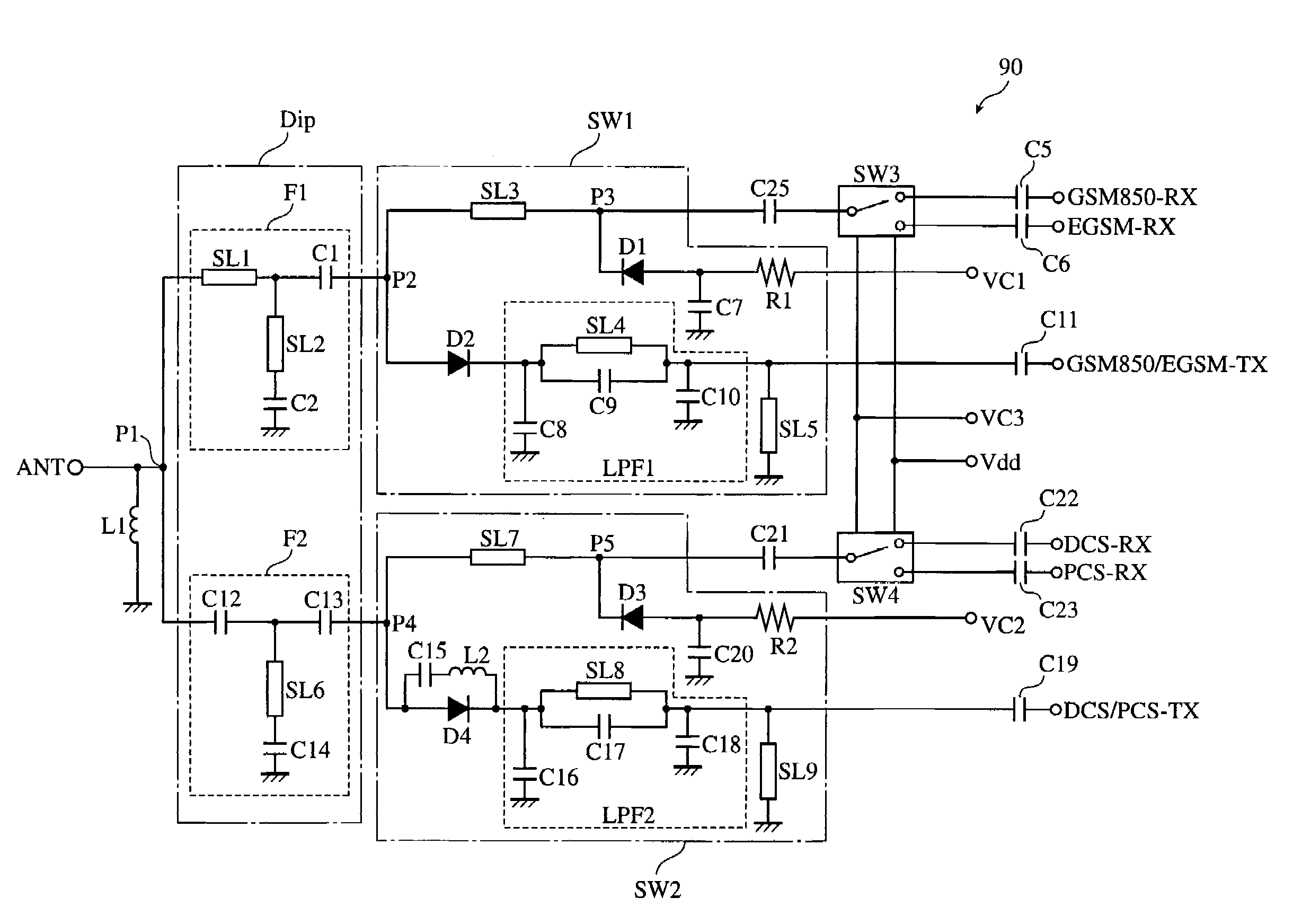
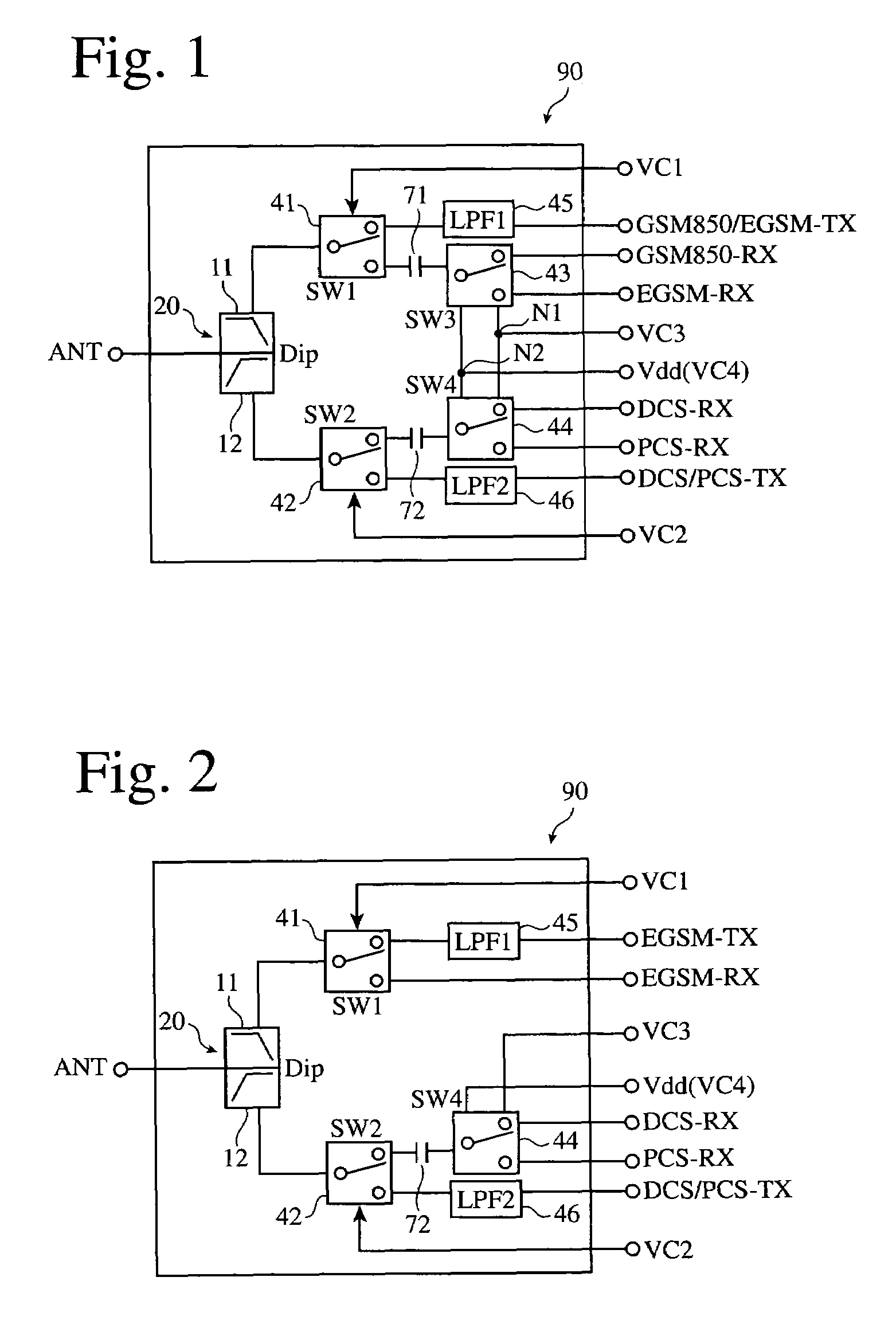
[0060]FIG. 1 is a block diagram showing the antenna switch circuit according to one embodiment of the present invention. In this embodiment, a first transmitting / receiving system handles a signal for GSM850 (transmission frequency: 824 to 849 MHz, receiving frequency: 869 to 894 MHz), a second transmitting / receiving system handles a signal for EGSM (transmission frequency: 880 to 915 MHz, receiving frequency: 925 to 960 MHz), a third transmitting / receiving system handles a signal for DCS (transmission frequency 1710 to 1785 MHz, receiving frequency: 1805 to 1880 MHz), and a fourth transmitting / receiving system handles a signal for PCS (transmission frequency: 1850 to 1910 MHz, receiving frequency 1930 to 1990 MHz). An antenna switch circuit comprises a function of properly switching the connection of a GSM850 / EGSM transmitting path, a GSM850 receiving path, an EGSM receiving path, a DCS / PCS transmitting path, a DCS receiving path and a PC...


PUM


Abstract

An antenna switch module connected to a common antenna for switching the connection of the antenna to a transmission circuit or a receiving circuit in plural transmitting / receiving systems having different passbands, comprising a diplexer circuit comprising a low-pass filter and a high-pass filter; a first switch circuit connected to the low-pass filter and for switching a transmitting line and a receiving line, a second switch circuit connected to the high-pass filter for switching a transmitting line and a receiving line; a third switch circuit connected to the first switch circuit for switching the receiving line from the first switch circuit; and a fourth switch circuit connected to the second switch circuit for switching the receiving line from the second switch circuit; at least part of transmission lines constituting LC circuits in the diplexer circuit and the first and second switch circuits being electrode patterns formed in a multilayer substrate constituted by plural dielectric layers; and chip elements constituting part of the LC circuits, diode elements constituting the first and second switch circuits, and semiconductor elements constituting the third and fourth switch circuits being mounted onto the multilayer substrate.

Description

FIELD OF THE INVENTION[0001]The present invention relates to an antenna switch circuit for switching signal paths of at least three frequency bands connected to a common antenna in a multiband mobile phone system adapted for different frequency bands such as GSM850, EGSM, DCS and PCS, and an antenna switch module comprising a plurality of such antenna switch circuits formed in a laminate.BACKGROUND OF THE INVENTION[0002]Because of rapid development of mobile phones, etc. worldwide, mobile phones utilizing plural frequency bands and plural communications systems have been put into practical use. Because they should be operated as multiband terminals adapted for different frequency bands and communications systems, they have complicated circuits, resulting in increase in the number of parts and their size and cost. Accordingly, the reduction of the number of parts and the sharing of parts are actively pursued by circuit integration.[0003]Because the sharing of a particularly large ant...

Claims


Application Information

Patent Timeline
Patent Type & Authority Patents(United States)
IPC IPC(8): H04B1/44H03H7/46H03H7/48H04B1/46H04B1/40H04B1/52
CPCH04B1/0057H04B1/006H04B1/44H04B1/406H04B1/52
Inventor YAMASHITA, TAKAHIROFUKAMACHI, KEISUKEKEMMOCHI, SHIGERU
Owner HITACHI METALS LTD
Learn More