
In-plane switching mode liquid crystal display device

a liquid crystal display and switching mode technology, applied in static indicating devices, optics, instruments, etc., can solve problems such as degrading picture quality, and achieve the effect of improving storage capacitance and preventing disclination

Active Publication Date: 2007-11-13
LG DISPLAY CO LTD
View PDF6 Cites 13 Cited by
  • Summary
  • Abstract
  • Description
  • Claims
  • Application Information

AI Technical Summary

Benefits of technology

The present invention is an IPS mode LCD device that solves problems of existing technology. It prevents disclination at bent portions of an electrode and improves storage capacitance. The device includes a gate line, a common electrode with a bent portion, a first disclination prevention pattern, a first supplementary capacitor electrode, a data line, a thin film transistor, a pixel electrode, and a second disclination prevention pattern. The technical effects of the invention are to prevent disclination and improve storage capacitance.

Problems solved by technology

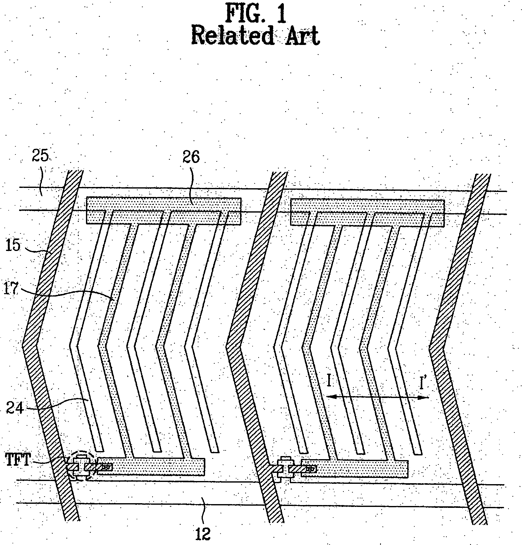
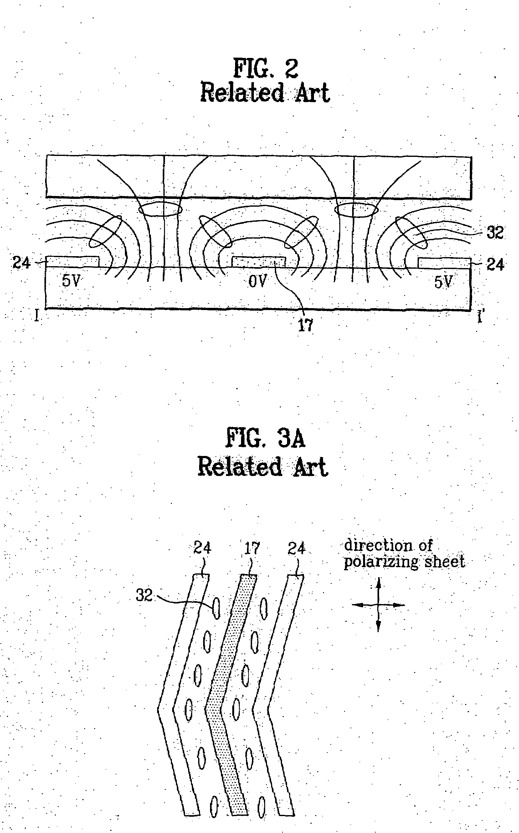
However, because the liquid crystal molecules 32 are aligned in the different directions in the bent portion ‘A’ of the electrode, a disclination line may generate light leakage which degrades the picture quality.

Method used


Image

  • In-plane switching mode liquid crystal display device
  • In-plane switching mode liquid crystal display device
  • In-plane switching mode liquid crystal display device

Examples


Embodiment Construction

[0032]Reference will now be made in detail to embodiments of the present invention, examples of which are illustrated in the accompanying drawings. Wherever possible, the same reference numbers will be used throughout the drawings to refer to the same or like parts.

[0033]Hereinafter, an IPS mode LCD device according to the present invention will be described with reference to the accompanying drawings.

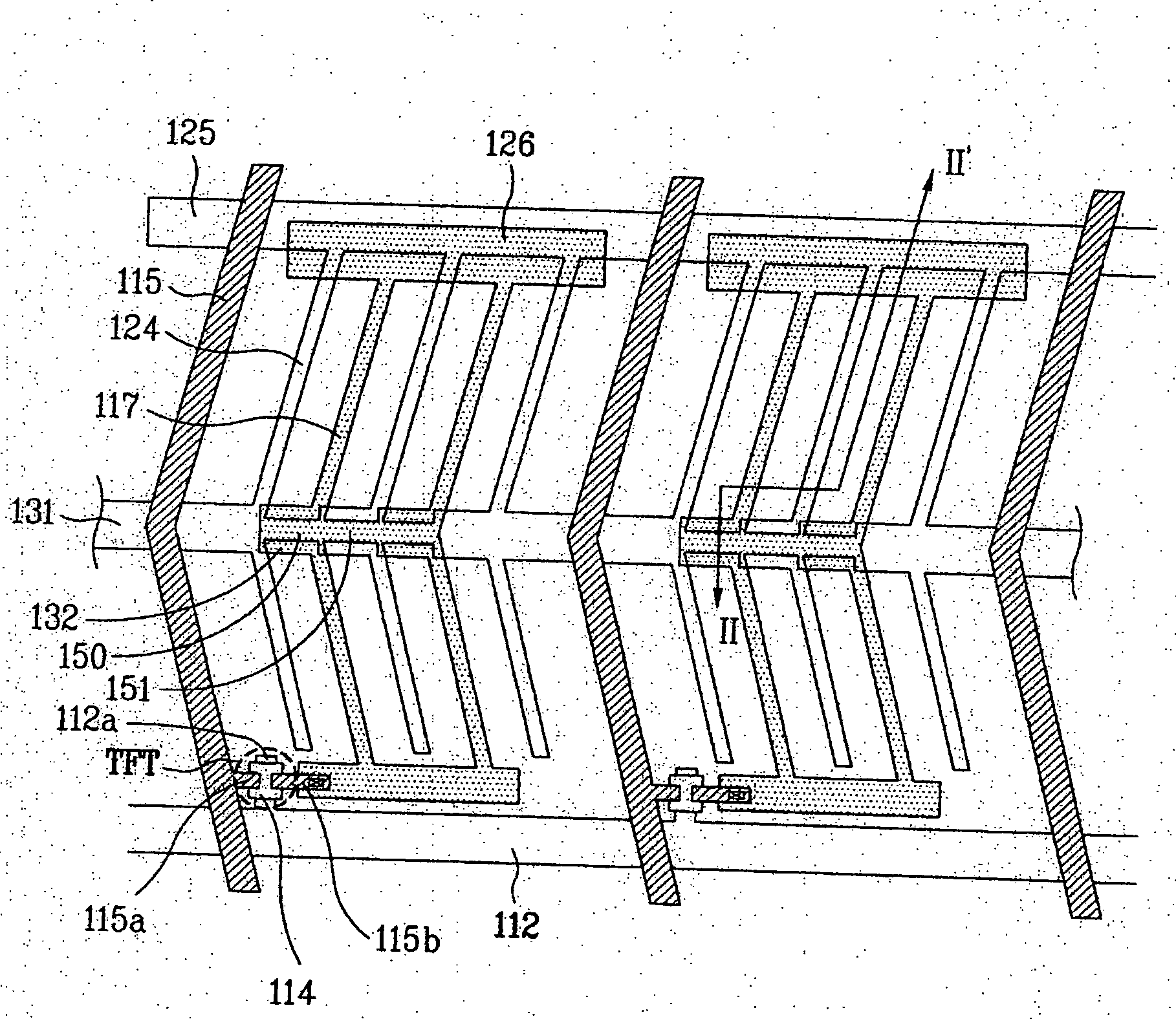
[0034]As shown in FIG. 4, a thin film transistor array substrate of an IPS mode LCD device according to the present invention includes a gate line 112, a data line 115, a thin film transistor TFT, a common line 125, a plurality of common electrodes 124, a plurality of pixel electrodes 117, and a capacitor electrode 126. The gate line 112 is formed in one direction on the thin film transistor array substrate, and the data line 115 is formed substantially perpendicular to the gate line 112 to define a pixel region. Also, the data line 115 is formed to have a bent structure. Then, the thi...


PUM

PropertyMeasurementUnit
sizeaaaaaaaaaa
weightaaaaaaaaaa
electric fieldaaaaaaaaaa

Abstract

An IPS mode LCD device includes a gate line on a substrate along one direction; a common electrode having a bent portion; a first disclination prevention pattern portion extended from the bent portion of the common electrode toward one side of the common electrode; a data line substantially perpendicular to the gate line; a thin film transistor at a crossing portion of the gate and data lines; a pixel electrode connected to a drain electrode of the thin film transistor, the pixel electrode having a bent portion and being formed substantially parallel to the common electrode; and a second disclination prevention pattern portion extended from a bent portion of the pixel electrode toward one side of the pixel electrode.

Description

[0001]This application claims the benefit of the Korean Application No. P2003-97619 filed on Dec. 26, 2003 and No. P2004-81393 filed on Oct. 12, 2004, which is hereby incorporated by reference for all purposes as if fully set forth herein.BACKGROUND OF THE INVENTION[0002]1. Field of the Invention[0003]The present invention relates to a liquid crystal display (LCD) device. More particularly, the present invention relates to an In-Plane Switching (IPS) mode LCD device.[0004]2. Discussion of the Related Art[0005]Liquid crystal display (LCD) devices have been actively studied and researched because of their advantageous characteristics such as high contrast ratio, gray level, high picture quality and low power consumption. The LCD device is especially suitable as an ultra-thin display device such as a wall-mountable television. The LCD device has also attracted great attention as a display device that can be substituted for CRTs because the LCD device has a thin profile, light weight an...

Claims


Application Information

Patent Timeline
Patent Type & Authority Patents(United States)
IPC IPC(8): G02F1/1343G02F1/133G02F1/1337G02F1/136G02F1/1362G02F1/1368H01L29/786
CPCG02F1/134363G02F2001/13373G02F1/136213G02F1/13373
Inventor KO, DOO HYUN
Owner LG DISPLAY CO LTD
Learn More