Liquid crystal display apparatus
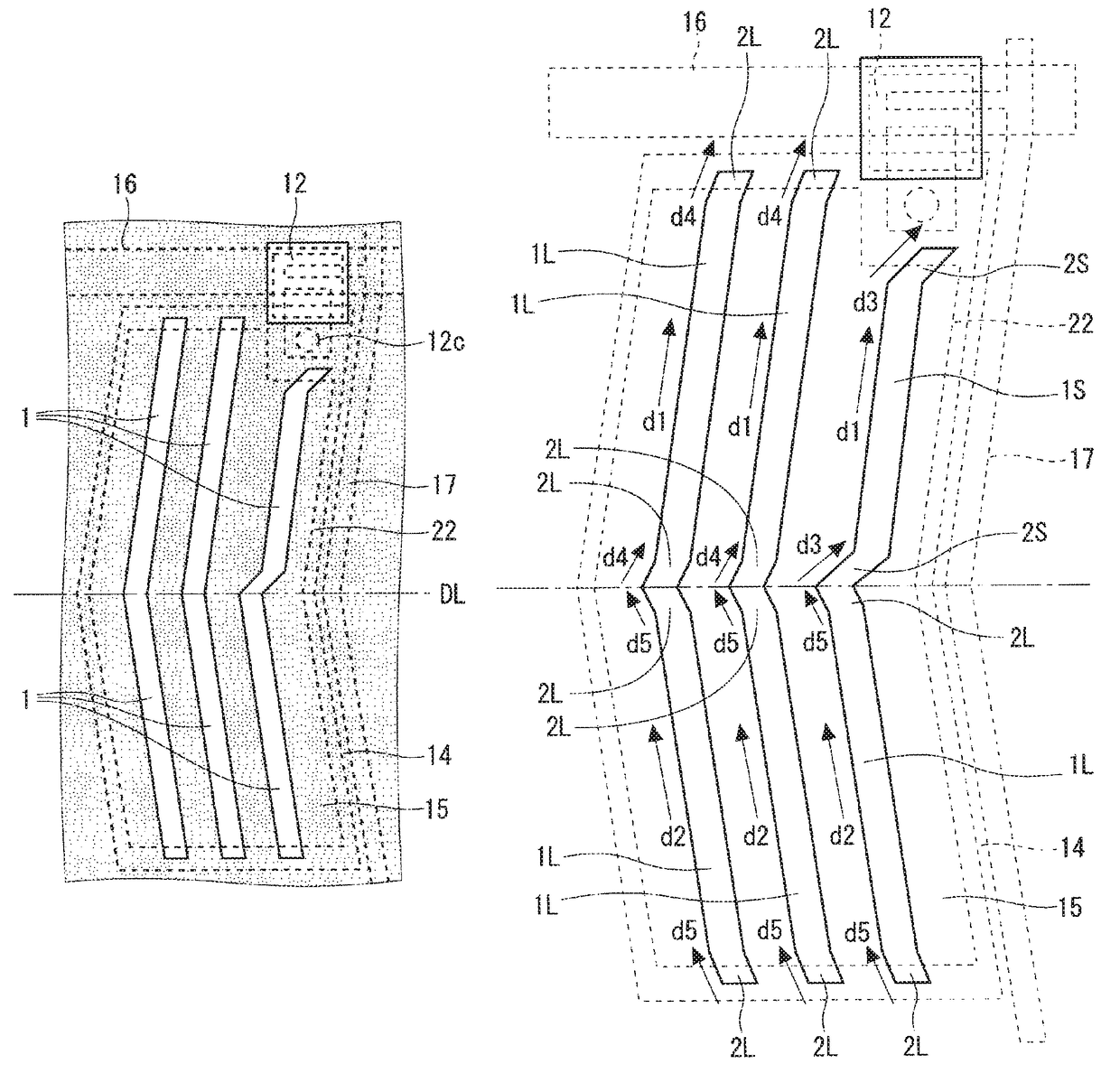
a technology of liquid crystal display and display device, which is applied in the direction of instruments, non-linear optics, optics, etc., can solve problems such as light leakage, and achieve the effect of minimizing the decrease of contrast ratio and preventing disclination
- Summary
- Abstract
- Description
- Claims
- Application Information
AI Technical Summary
Benefits of technology
Problems solved by technology
Method used
Image
Examples
first preferred embodiment
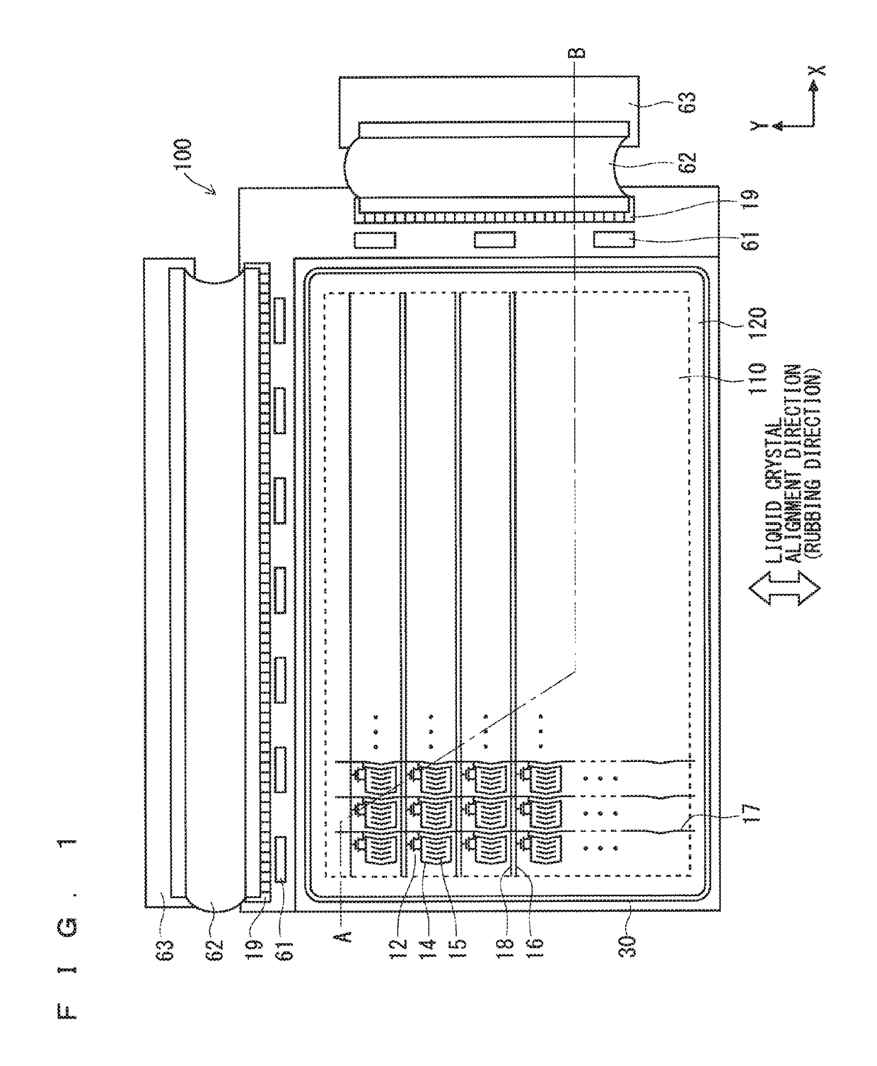
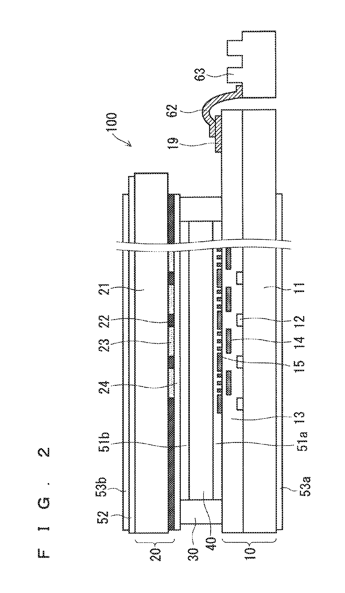
[0021]FIGS. 1 and 2 are schematic diagrams of a liquid crystal panel forming a liquid crystal display apparatus according to a first preferred embodiment of the present invention. FIG. 1 is a plan view illustrating the liquid crystal panel in its entirety. FIG. 2 is a cross-sectional view taken along line A-B in FIG. 1. The present preferred embodiment illustrates an example in which the present invention is applied to a liquid crystal panel in a transverse electric field mode that uses thin film transistors (TFTs) as switching elements of individual pixels, and particularly applied to a liquid crystal panel in a FFS mode.
[0022]As illustrated in FIGS. 1 and 2, a liquid crystal panel 100 includes a TFT array substrate 10 (hereinafter referred to as an “array substrate 10”), a color filter substrate 20, and a liquid crystal layer 40 sealed between the array substrate 10 and the color filter substrate 20 with a sealant 30.
[0023]The sealant 30 surrounds a display region 110 where pixels...
second preferred embodiment
[0057]FIG. 8 is a schematic diagram of a liquid crystal panel forming a liquid crystal display apparatus according to a second preferred embodiment. The liquid crystal display apparatus according to the second preferred embodiment is basically configured similarly to the liquid crystal display apparatus according to the first preferred embodiment except that an extending direction of slits 1 disposed in an individual counter electrode 15 is a row direction (x direction) of pixels. As previously described, the liquid crystal alignment direction (rubbing direction) of the alignment films 51a and 52b (FIG. 2) is along the extending direction of the slits 1 of the counter electrode 15. Hence, the x direction is the liquid crystal alignment direction.
[0058]FIGS. 9 and 10 are diagrams illustrating configurations of the pixel of the liquid crystal panel according to the second preferred embodiment. FIG. 9 is a plan view of one pixel with an array substrate 10 and a color filter substrate 2...
PUM
| Property | Measurement | Unit |
|---|---|---|
| bend angle | aaaaa | aaaaa |
| angle | aaaaa | aaaaa |
| electric field | aaaaa | aaaaa |
Abstract
Description
Claims
Application Information
 - R&D
- Intellectual Property
- Life Sciences
- Materials
- Tech Scout
- Unparalleled Data Quality
- Higher Quality Content
- 60% Fewer Hallucinations
Browse by: Latest US Patents, China's latest patents, Technical Efficacy Thesaurus, Application Domain, Technology Topic, Popular Technical Reports.
© 2025 PatSnap. All rights reserved.Legal|Privacy policy|Modern Slavery Act Transparency Statement|Sitemap|About US| Contact US: help@patsnap.com


