Active device array substrate and liquid crystal display panel
a technology of active devices and array substrates, which is applied in the field of active device array substrates and liquid crystal display panels, can solve the problems of reducing the image quality of the lcd panel, and achieve the effect of effectively preventing the dislocation of liquid crystal molecules
- Summary
- Abstract
- Description
- Claims
- Application Information
AI Technical Summary
Benefits of technology
Problems solved by technology
Method used
Image
Examples
first embodiment
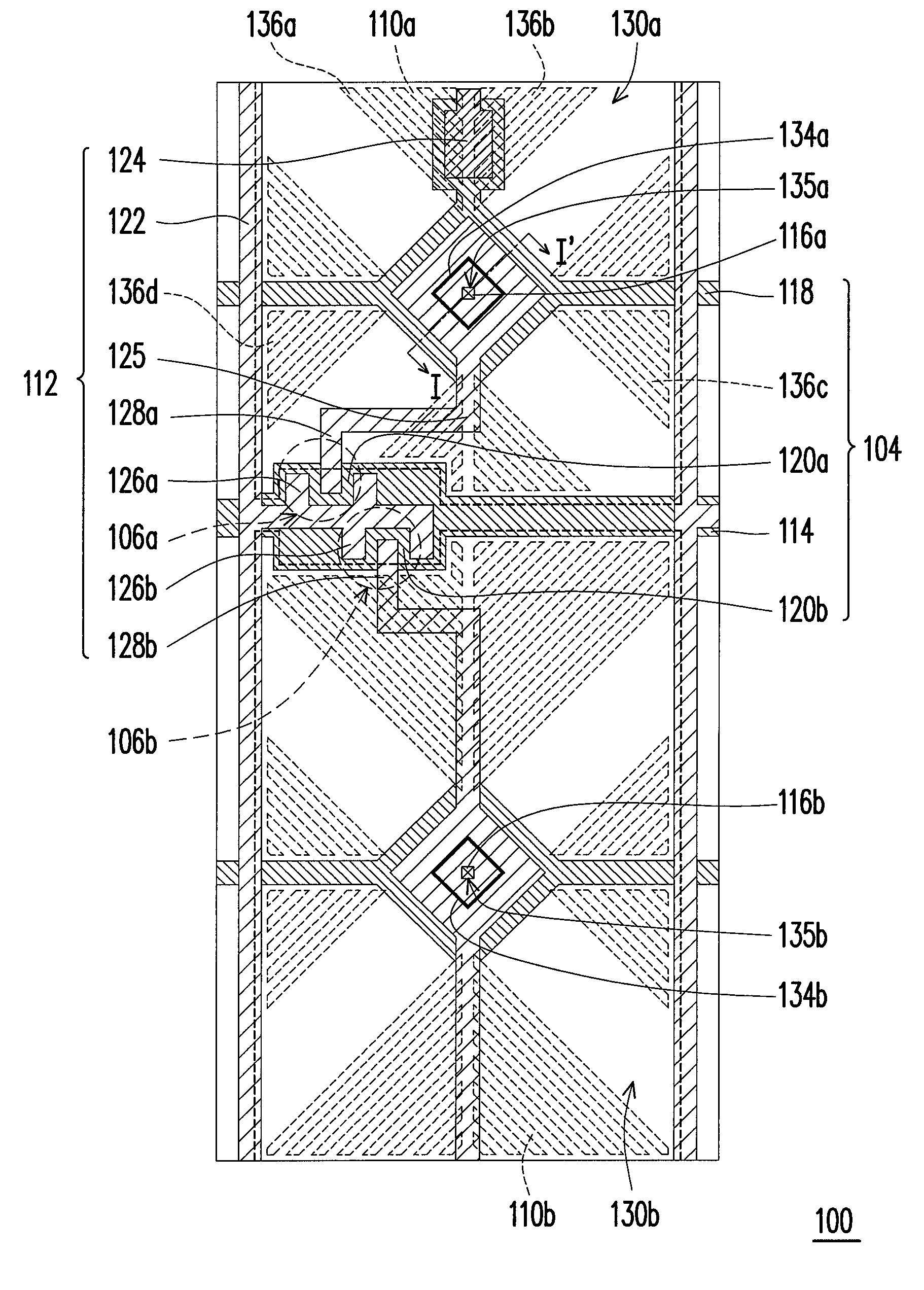
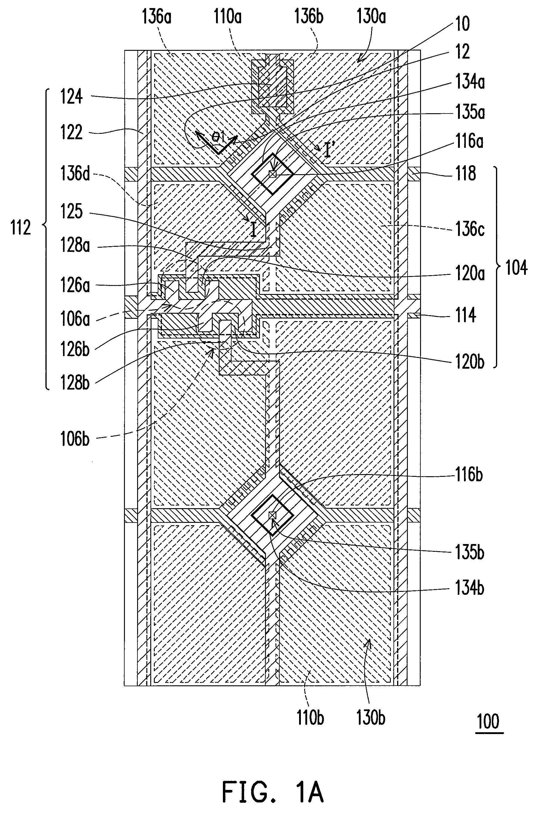
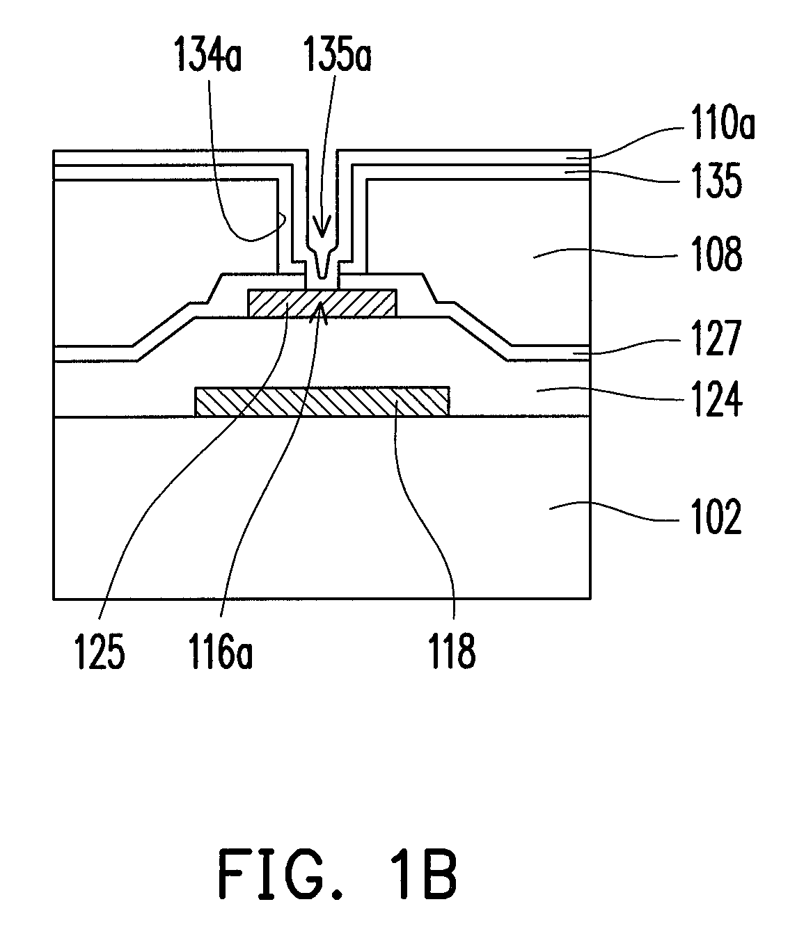
[0037]FIG. 1A is a schematic top view illustrating an active device array substrate according to a first embodiment of the invention. FIG. 1B is a schematic cross-sectional view taken along a section line I-I′ depicted in FIG. 1A. In the embodiment, only one pixel region is depicted for the purpose of explanation. The pixel region has two pixel electrodes, and two active devices are correspondingly disposed. Certainly, based on actual design demands, one or more pixel electrodes can be disposed in the pixel region, and the number of the active devices is correspondingly decided.
[0038]To elaborate the invention with reference to FIGS. 1A and 1B with clarity, some film layers including a color filter layer 108, a dielectric layer 124, and a passivation layer 127 are omitted in FIG. 1A. The active device array substrate 100 includes a substrate 102, a patterned conductive layer 104, active devices 106a and 106b, a color filter layer 108, pixel electrodes 110a and 110b, and a patterned ...
second embodiment
[0043]In view of the fact that the terrain around the openings of the color filter layer gives rise to sufficient alignment of the liquid crystal molecules, the fine slits around the openings of the color filter layer can be omitted in this embodiment. That is to say, it is not necessary to form the fine slits around the openings in the pixel electrodes according to this embodiment, and light emitting efficiency of the display panel can be further improved. FIG. 2 is a schematic top view illustrating an active device array substrate according to this embodiment of the invention. As shown in FIG. 2, pixel electrodes 110a′ and 110b′ do not have fine slits around the openings 134a and 134b.
third embodiment
[0044]FIG. 3 is a schematic top view illustrating an active device array substrate according to a third embodiment of the invention. In the embodiment, only one pixel region is depicted for the purpose of explanation. The pixel region has two pixel electrodes, and two active devices are correspondingly disposed. Certainly, based on actual design demands, one or more pixel electrodes can be disposed in the pixel region, and the number of the active devices is correspondingly decided, which should not be construed as limited to the embodiments set forth herein.
[0045]Besides, based on the same principle described in the first embodiment, extension directions of fine slits on pixel electrodes and extension directions of sides of openings exposing pixel regions in light shielding layers together form included angles ranging from 60° to 90° in this embodiment. Thereby, after an active device array substrate and an opposite substrate are combined to form an LCD panel, liquid crystal molecu...
PUM
| Property | Measurement | Unit |
|---|---|---|
| included angle | aaaaa | aaaaa |
| dielectric constant | aaaaa | aaaaa |
| operational temperature | aaaaa | aaaaa |
Abstract
Description
Claims
Application Information
 - R&D
- Intellectual Property
- Life Sciences
- Materials
- Tech Scout
- Unparalleled Data Quality
- Higher Quality Content
- 60% Fewer Hallucinations
Browse by: Latest US Patents, China's latest patents, Technical Efficacy Thesaurus, Application Domain, Technology Topic, Popular Technical Reports.
© 2025 PatSnap. All rights reserved.Legal|Privacy policy|Modern Slavery Act Transparency Statement|Sitemap|About US| Contact US: help@patsnap.com


