
Solid-state image pickup device and device driving control method for solid-state image pickup

a technology of solid-state image and pickup device, which is applied in the direction of radio frequency controlled devices, television system scanning details, television systems, etc., can solve the problems of quasi-blooming phenomenon, similar to the blooming phenomenon, and suppress the quasi-blooming phenomenon. , to achieve the effect of reducing picture degradation, suppressing the quasi-blooming phenomenon, and reducing the blooming phenomenon

Active Publication Date: 2007-09-18
SONY CORP
View PDF7 Cites 188 Cited by
  • Summary
  • Abstract
  • Description
  • Claims
  • Application Information

AI Technical Summary

Benefits of technology

[0015]The present invention has been made in view of the above, and it is accordingly an object of the present invention to provide a solid-state image pickup device and a driving control method for the solid-state image pickup device that make it possible to suppress the blooming phenomenon and the quasi-blooming phenomenon with a simple structure and a simple control method.
[0034]Further, the charge generating section does not need to be reset when the unnecessary charge discharging gate section is in an on state. That is, control may be effected such that a charge well is formed with the charge generating section at a center of the well.
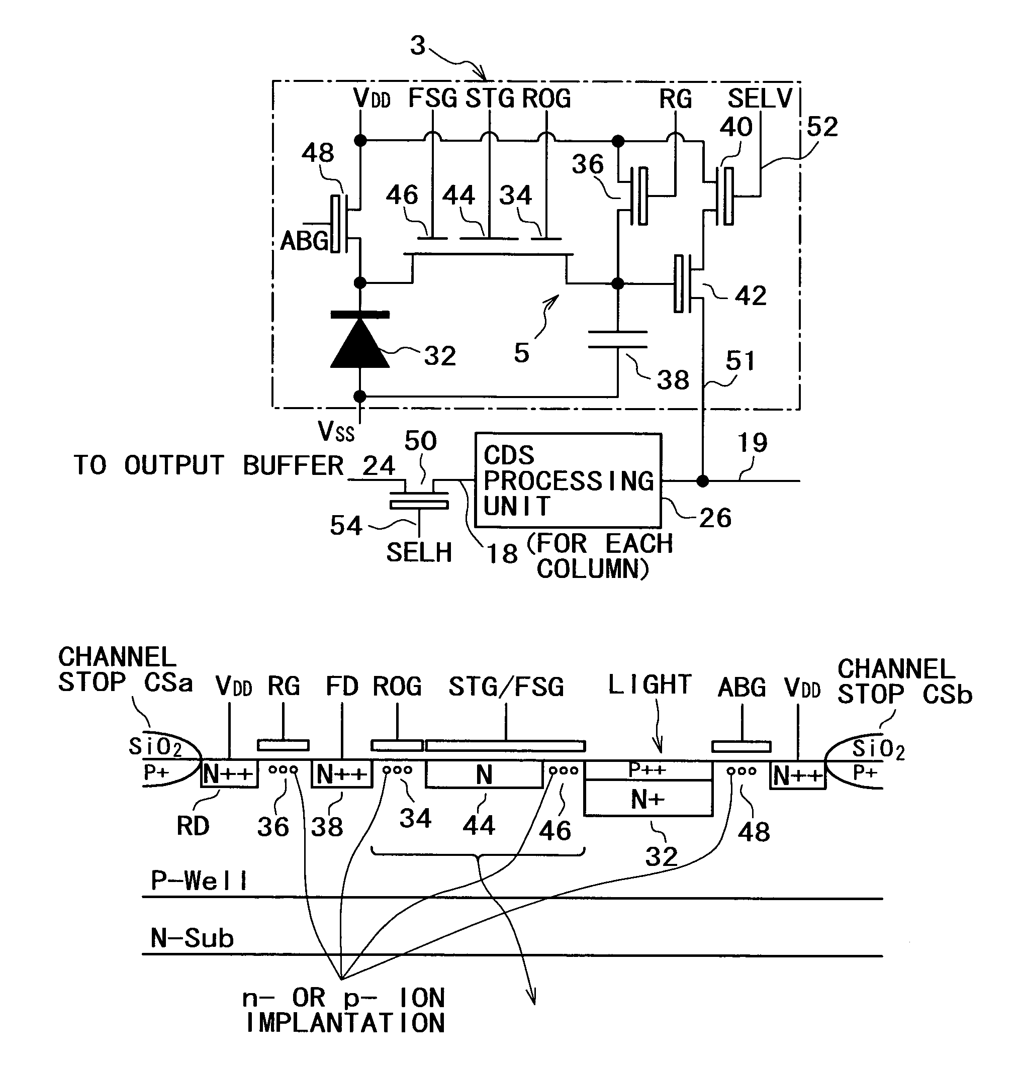
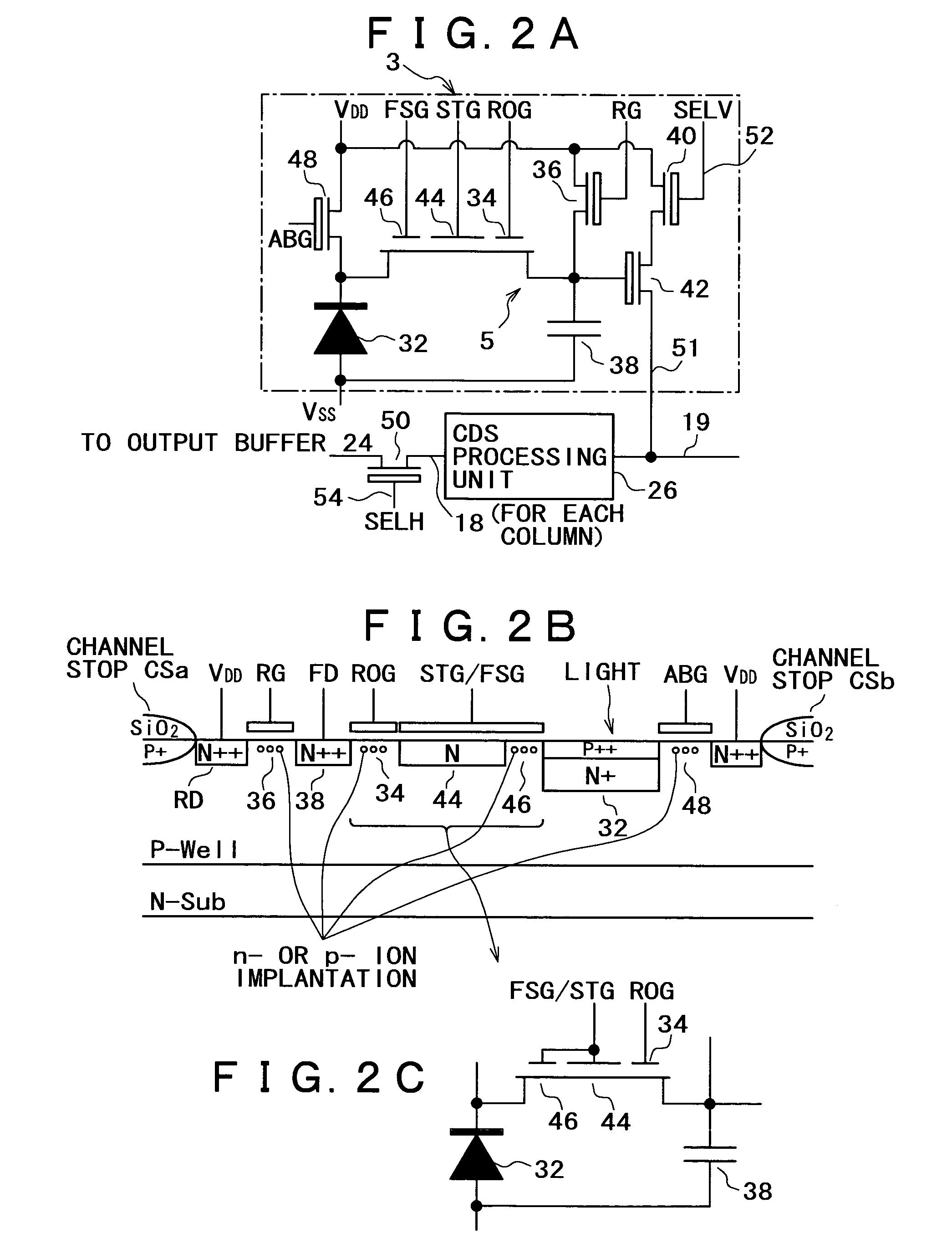
[0036]Thereby, while the unnecessary charge discharging gate section is turned off during a period of exposure accumulation of the charge generating section so as not to affect the accumulation of signal charge, an excess charge generated by irradiating the charge generating section with excessive light during the period of exposure accumulation can be discharged over the unnecessary charge discharging gate section to the unnecessary charge drain section. It is thus possible to reduce picture degradation due to the excess charge. That is, it is possible to reduce the blooming phenomenon in the period of exposure accumulation.
[0037]On the other hand, by turning on the unnecessary charge discharging gate section during a period other than the period of exposure accumulation, it is possible to prevent unnecessary charge generated in the charge generating section during this period from entering the charge storage section. That is, it is possible to suppress the quasi-blooming phenomenon in the period other than the period of exposure accumulation.
[0038]Thus, according to the present invention, it is possible to suppress effects of unnecessary charge caused by the blooming phenomenon and the quasi-blooming phenomenon with a simple configuration in which the unnecessary charge discharging gate section is provided for each pixel.

Problems solved by technology

However, when the shutter speed is set fast to a degree that the shutter speed is not so different from a horizontal scanning period of the shutter speed, the difference in the accumulation time appears as shading in a line direction (horizontal direction) in an image, thus presenting a problem.
However, when intense light enters the photoelectric converting element of the charge generating section, a so-called “blooming phenomenon” becomes a problem, in which phenomenon a charge more than a maximum amount of charge that can be accumulated in the photoelectric converting element is generated, and the charge overflows the photoelectric converting element through a transfer gate or a channel stop region into the pixel signal generating section or a charge generating section within an adjacent pixel or the like.
Furthermore, when a charge generated as a result of light entering the photoelectric converting element after a signal charge is transferred to the charge storage section overflows into the charge storage section, a problem (quasi-blooming phenomenon) similar to the blooming phenomenon occurs.

Method used


Image

  • Solid-state image pickup device and device driving control method for solid-state image pickup
  • Solid-state image pickup device and device driving control method for solid-state image pickup
  • Solid-state image pickup device and device driving control method for solid-state image pickup

Examples


first embodiment

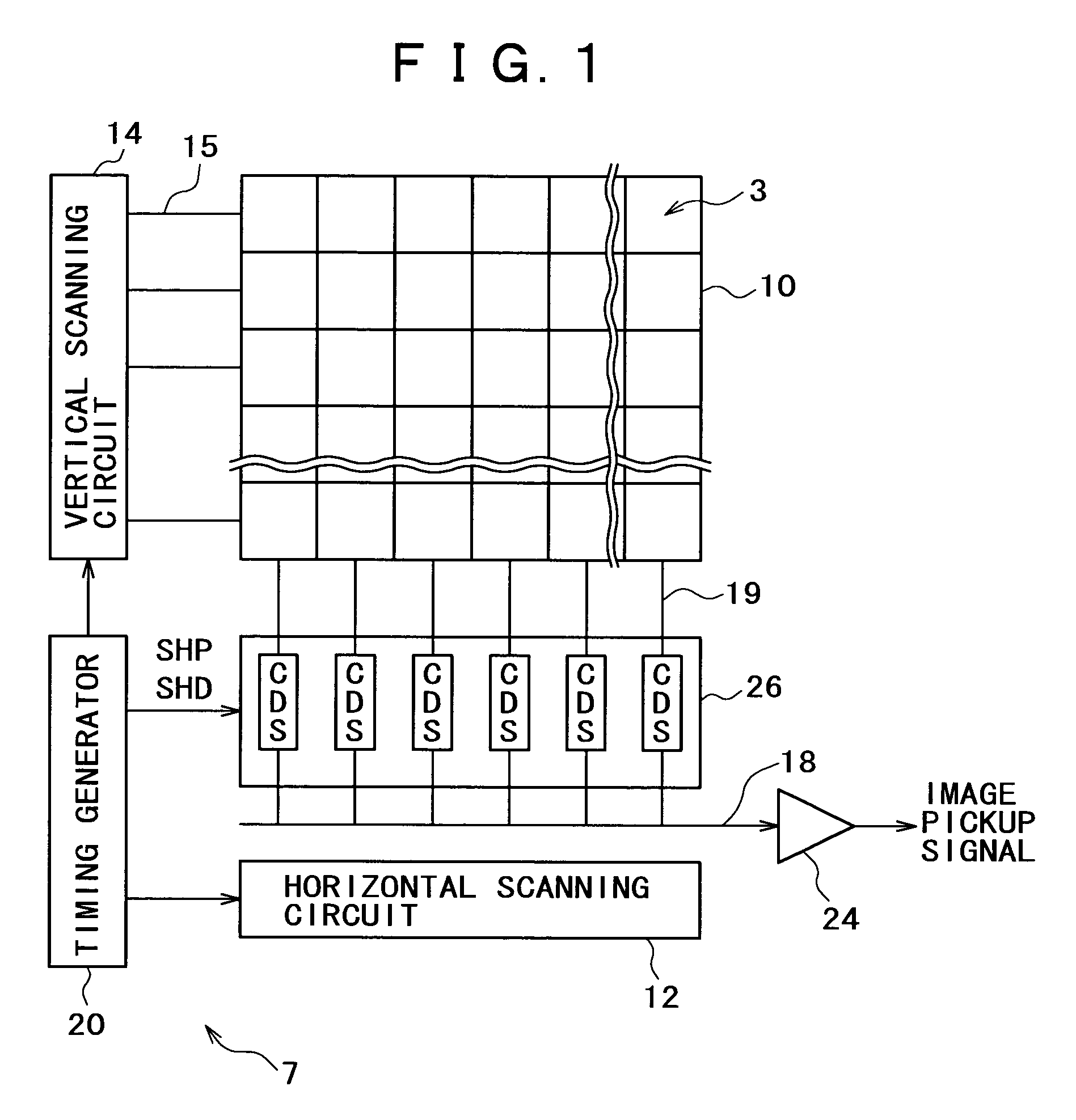
[0051]FIG. 1 is a schematic diagram of configuration of a solid-state image pickup device according to the present invention. The solid-state image pickup device 1 is a column type solid-state image pickup device in which pixels are arranged in a form of rows and columns, signal outputs from the pixels are outputted as voltage signals, and a CDS (Correlated Double Sampling) processing function unit is provided for each column.

[0052]Specifically, as shown in FIG. 1, the solid-state image pickup device 1 includes an image pickup unit 10 in which a plurality of unit pixels 3 are arranged in the form of rows and columns, a driving control unit 7 provided on the outside of the image pickup unit 10, and a CDS processing unit 26. A horizontal scanning circuit 12 and a vertical scanning circuit 14, for example, are provided as the driving control unit 7. While FIG. 1 does not show a part of the rows and columns for simplicity, several tens to several thousands of pixels are arranged in each...

second embodiment

[0162]FIGS. 10A and 10B are diagrams showing a detailed example of a unit pixel 3 in the image pickup unit 10 of the solid-state image pickup device 1 shown in FIG. 1. FIG. 10A is a diagram of a fundamental equivalent circuit of the unit pixel 3 (partly including a peripheral section); and FIG. 10B is a sectional view of the unit pixel 3.

[0163]While the unit pixel 3 according to the first embodiment is characterized by including the floating diffusion 38 and the charge storage section 44 as a charge storage part for retaining a signal charge generated in the charge generating section 32 (photodiode PD) for a certain period after the signal charge is transferred simultaneously in all the pixels to realize the global shutter function, the unit pixel 3 according to the second embodiment is characterized in that the function of the charge storage section 44 is performed by a floating diffusion 38 alone. In this case, a readout gate ROG performs the function of the frame shift gate FSG.

[...


PUM


Abstract

Disclosed herein is a solid-state image pickup device including: a plurality of unit pixels each having: a charge generating section for generating a charge, a charge storage section for storing the charge generated by the charge generating section, a transfer gate section disposed between the charge generating section and the charge storage section for transferring the charge generated by the charge generating section to the charge storage section, and a pixel signal generating section for generating a pixel signal corresponding to the charge stored in the charge storage section; an unnecessary charge discharging gate section in each the unit pixel, switchable to block a flow of an unnecessary charge that is generated in the charge generating section and does not contribute to image formation, according to height of an electric barrier; and an unnecessary charge drain section disposed on an opposite side of the unnecessary charge discharging gate section from the charge generating section for receiving the unnecessary charge swept out of the charge generating section through the unnecessary charge discharging gate section.

Description

[0001]This application claims priority to Japanese Patent Application Numbers JP2002-271025 filed Sep. 18, 2002 which is incorporated herein by reference.BACKGROUND OF THE INVENTION[0002]The present invention relates to a solid-state image pickup device formed with an image pickup element having a plurality of unit pixels arranged therein and a driving control method for the solid-state image pickup device, and more particularly to a technique for discharging unnecessary charge in a solid-state image pickup device of a MOS type, a CMOS type or the like in which a pixel signal from a unit pixel is read by address control.[0003]As solid-state image pickup devices of a system that reads pixel signals from charge generating sections including a plurality of photoelectric converting elements (photodiodes or the like) within an image pickup unit by controlling a pixel position by address control, there are solid-state image pickup devices of a MOS type and a CMOS type (which will hereinaf...

Claims


Application Information

Patent Timeline
IPC IPC(8): H04N3/14H04N5/335H01L27/146H04N5/353H04N5/357H04N5/359H04N5/363H04N5/369H04N5/374
CPCH01L27/14609H01L27/14643H04N5/3594H04N5/37452H04N25/623H04N25/771
Inventor IIZUKA, TETSUYAUENO, TAKAHISA
Owner SONY CORP
Learn More