Thin film transistor substrate and manufacturing method thereof
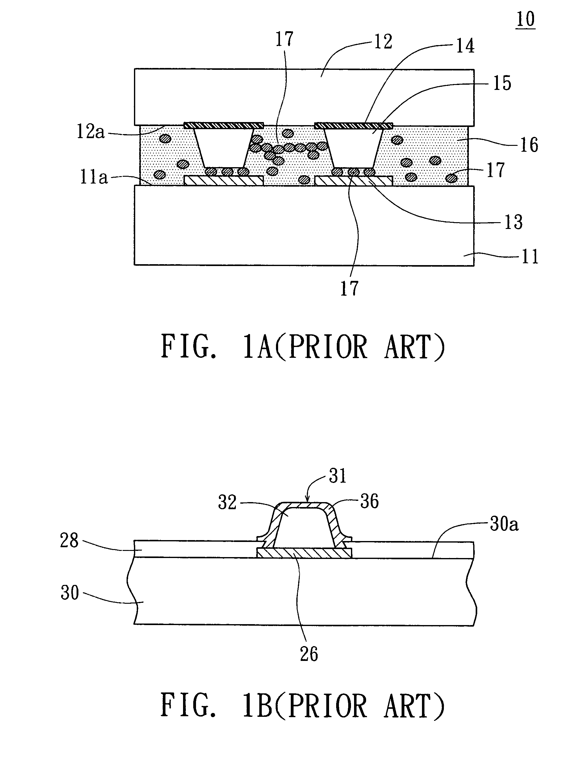
a technology of thin film transistors and manufacturing methods, which is applied in the direction of semiconductor devices, semiconductor/solid-state device details, electrical apparatus, etc., can solve the problems of difficult control of the height of composite bumps b>31/b> on the chip b>30/b>, affecting the electrical quality of the semiconductor structure, and difficult to control well the height of composite bumps b>10/b>, so as to prevent uneven surface, save materials, high quality bump bump
- Summary
- Abstract
- Description
- Claims
- Application Information
AI Technical Summary
Benefits of technology
Problems solved by technology
Method used
Image

Examples
example 1
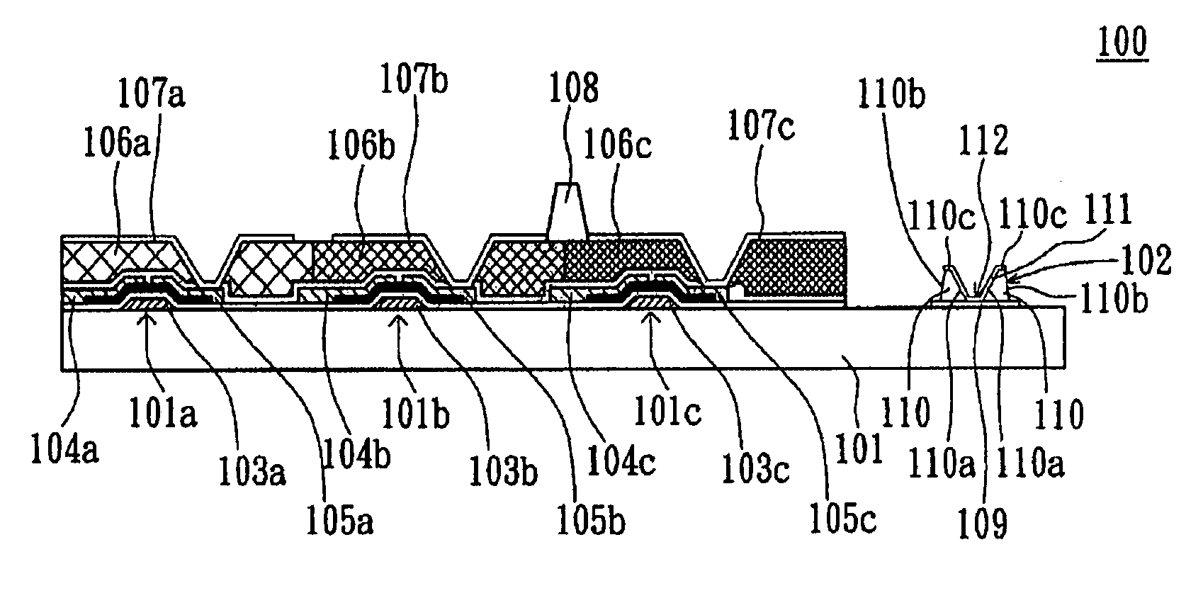
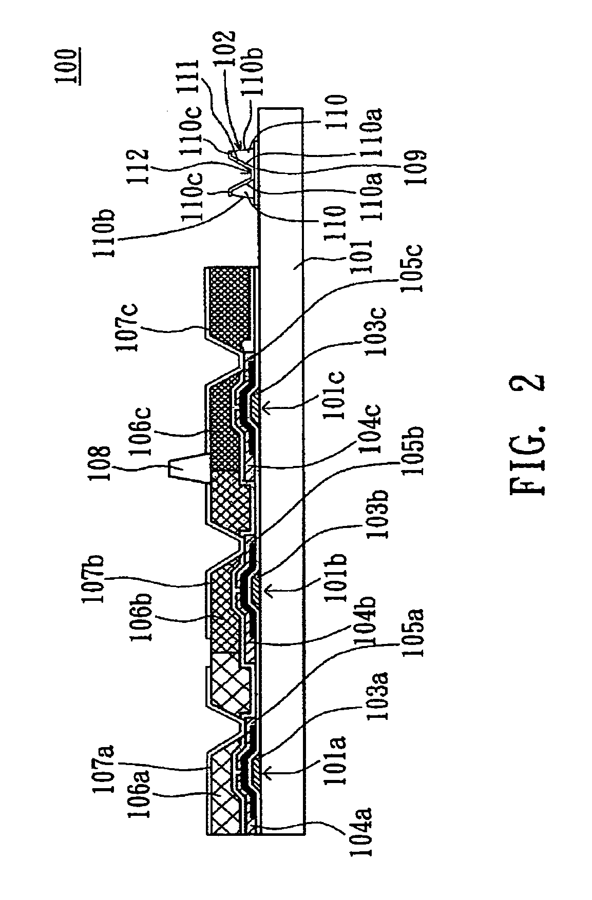
[0026]Referring to FIG. 2, FIG. 4A to FIG. 4F together, FIG. 4A to FIG. 4F are flow lateral views of the TFT substrate manufacturing method according to the first example of the preferred embodiment of the present invention. At first, in FIG. 4A, a glass substrate 101 is provided, and a first metal layer is formed on the glass substrate 101. The part of first metal layer is then removed so that the gate electrodes 103a, 103b and 103c, and the electrode pad 109 are formed on the glass substrate 101. Then, in FIG. 4B, the source electrode 104a and the drain electrode 105a are formed on the gate electrode 103a, the source electrode 104b and the drain electrode 105b are formed on the gate electrode 103b, and the source electrode 104c and the drain electrode 105c are formed on the gate electrode 103c. Therefore, the gate electrodes 103a, 103b and 103c, the source electrodes 104a, 104b and 104c, the drain electrodes 105a, 105b and 105c make up the TFTs 101a, 101b and 101c, respectively. A...
example 2
[0028]Referring to FIG. 2, FIG. 5A to FIG. 5F together, FIGS. 5A to 5F are flow lateral views of the TFT substrate manufacturing method according to the second example of the preferred embodiment of the present invention. At first, in FIG. 5A, a glass substrate 101 is provided, and a first metal layer is formed on the glass substrate 101. The part of first metal layer is then removed so that the gate electrodes 103a, 103b and 103c are formed on the glass substrate 101. Then, in FIG. 5B, a second metal layer is formed on the glass substrate 101, and the second metal layer covers the gate electrodes 103a, 103b and 103c. The part of second metal layer is removed, and the source electrodes 104a, 104b and 104c, the drain electrodes 105a, 105b and 105c, and the electrode pad 109 are formed. Besides, the source electrode 104a and the drain electrode 105a are formed on the gate electrode 103a, the source electrode 104b and the drain electrode 105b are formed on the gate electrode 103b, and ...
example 3
[0030]Referring to FIG. 2, FIG. 6A to FIG. 6F together, FIG. 6A to 6F are flow lateral views of the TFT substrate manufacturing method according to the third example of the preferred embodiment of the present invention. At first, in FIG. 6A, a glass substrate 101 is provided, and a first metal layer is formed on the glass substrate 101. The part of first metal layer is then removed so that the gate electrodes 103a, 103b and 103c, and the bottom layer 109a of the electrode pad are formed on the glass substrate 101. Then, in FIG. 6B, a second metal layer is formed on the glass substrate 101, and the second metal layer covers the gate electrodes 103a, 103b and 103c, and the bottom layer 109a of the electrode pad. The part of second metal layer is removed, and the source electrodes 104a, 104b and 104c, the drain 105a, 105b and 105c, and the top layer 109b of the electrode pad are formed. Besides, the source electrode 104a and the drain electrode 105a are formed on the gate electrode 103...
PUM
| Property | Measurement | Unit |
|---|---|---|
| conductive | aaaaa | aaaaa |
| sizes | aaaaa | aaaaa |
| electrical quality | aaaaa | aaaaa |
Abstract
Description
Claims
Application Information
 - R&D
- Intellectual Property
- Life Sciences
- Materials
- Tech Scout
- Unparalleled Data Quality
- Higher Quality Content
- 60% Fewer Hallucinations
Browse by: Latest US Patents, China's latest patents, Technical Efficacy Thesaurus, Application Domain, Technology Topic, Popular Technical Reports.
© 2025 PatSnap. All rights reserved.Legal|Privacy policy|Modern Slavery Act Transparency Statement|Sitemap|About US| Contact US: help@patsnap.com