Ground-enhanced semiconductor package and lead frame for the same

Active Publication Date: 2007-06-12
SILICONWARE PRECISION IND CO LTD
View PDF14 Cites 24 Cited by
  • Summary
  • Abstract
  • Description
  • Claims
  • Application Information

AI Technical Summary

Benefits of technology

[0009]An objective of the present invention is to provide a ground-enhanced semiconductor package and a lead frame for the same, which can prevent ground areas thereof from deformation under a high-temperature condition.
[0010]Another objective of the present invention is to provide a ground-enhanced semiconductor package and a lead frame for the same, to eliminate difficult bonding of ground wires.
[0011]Still another objective of the present invention is to provide a ground-enhanced semiconductor package and a lead frame for the same, to avoid breaking of ground wires.
[0012]A further objective of the present invention is to provide a ground-enhanced semiconductor package and a lead frame for the same, in which thermal stresses on ground areas thereof can be released.
[0013]A further objective of the present invention is to provide a ground-enhanced semiconductor package and a lead frame for the same, for reducing residual stresses on the lead frame during fabrication processes.
[0016]Therefore, in the use of the above ground-enhanced semiconductor package and lead frame proposed by the present invention, as the ground portions arranged on the lateral sides of the tie bars or on the side edges of the die pad are not interconnected, thermal stresses generated under a high temperature condition can be desirably released through the ground portions without causing deformation thereof thereby assuring the grounding performance.

Problems solved by technology

However, since the ground wires are usually bonded to peripheral areas on the die pad, in the case of delamination occurring between the die pad and the encapsulation body due to mismatch in coefficient of thermal expansion (CTE) thereof, the ground wires tend to break easily and degrade the electricity performance.
Such a drawback becomes more severe in an exposed-pad type package where the occurrence of delamination between the die pad and the encapsulation body is increased due to relatively weaker adhesion therebetween.
However, such a multi-layer lead frame is rather complex in structure which is not material-effective to fabricate, thereby leading to a burden for manufacture and costs of the semiconductor package as well as not in favor of large-scale production.
This thermal deformation is caused by thermal expansion of metallic material making the ground ring which is constrained within or not able to be released from the continuous ring structure, and thereby damages the planarity of the ground ring.
The deformed ground ring also increases the difficulty in bonding the ground wires, or the ground wires may subject to breaking by the deformation, making the electricity performance undesirably degraded.
Besides, during a stamping process for fabricating the lead frame having the continuous ground ring, the stamping force may be left to form residual stresses in the ground ring, which also leads to deformation of the ring structure under a subsequent high-temperature environment.
Namely, the provision of the S-shaped tie bars still fails to solve the problem of ground-ring deformation.

Method used


Image

  • Ground-enhanced semiconductor package and lead frame for the same
  • Ground-enhanced semiconductor package and lead frame for the same
  • Ground-enhanced semiconductor package and lead frame for the same

Examples


second embodiment

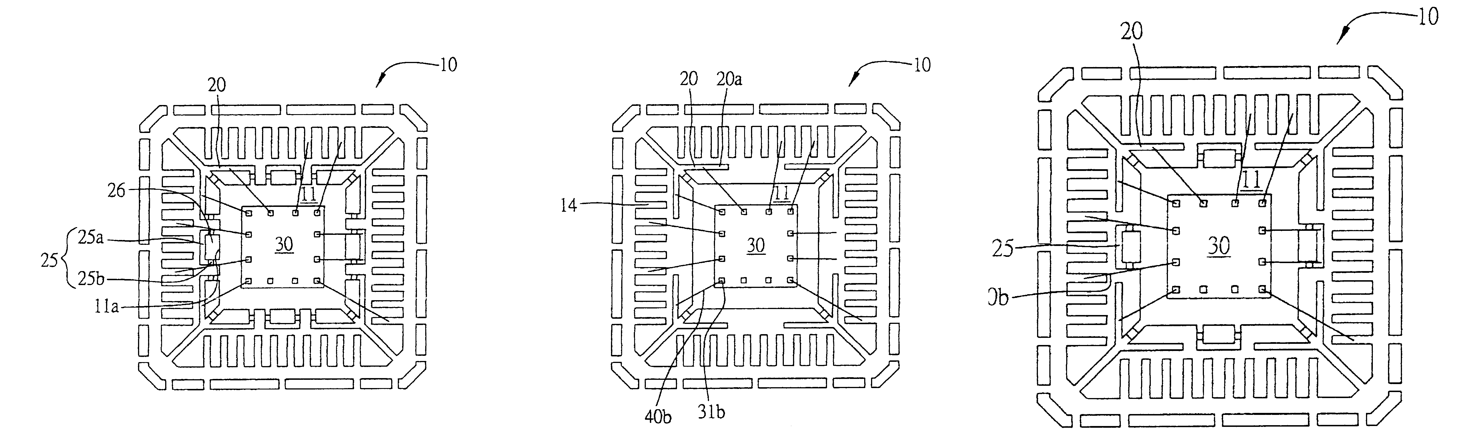
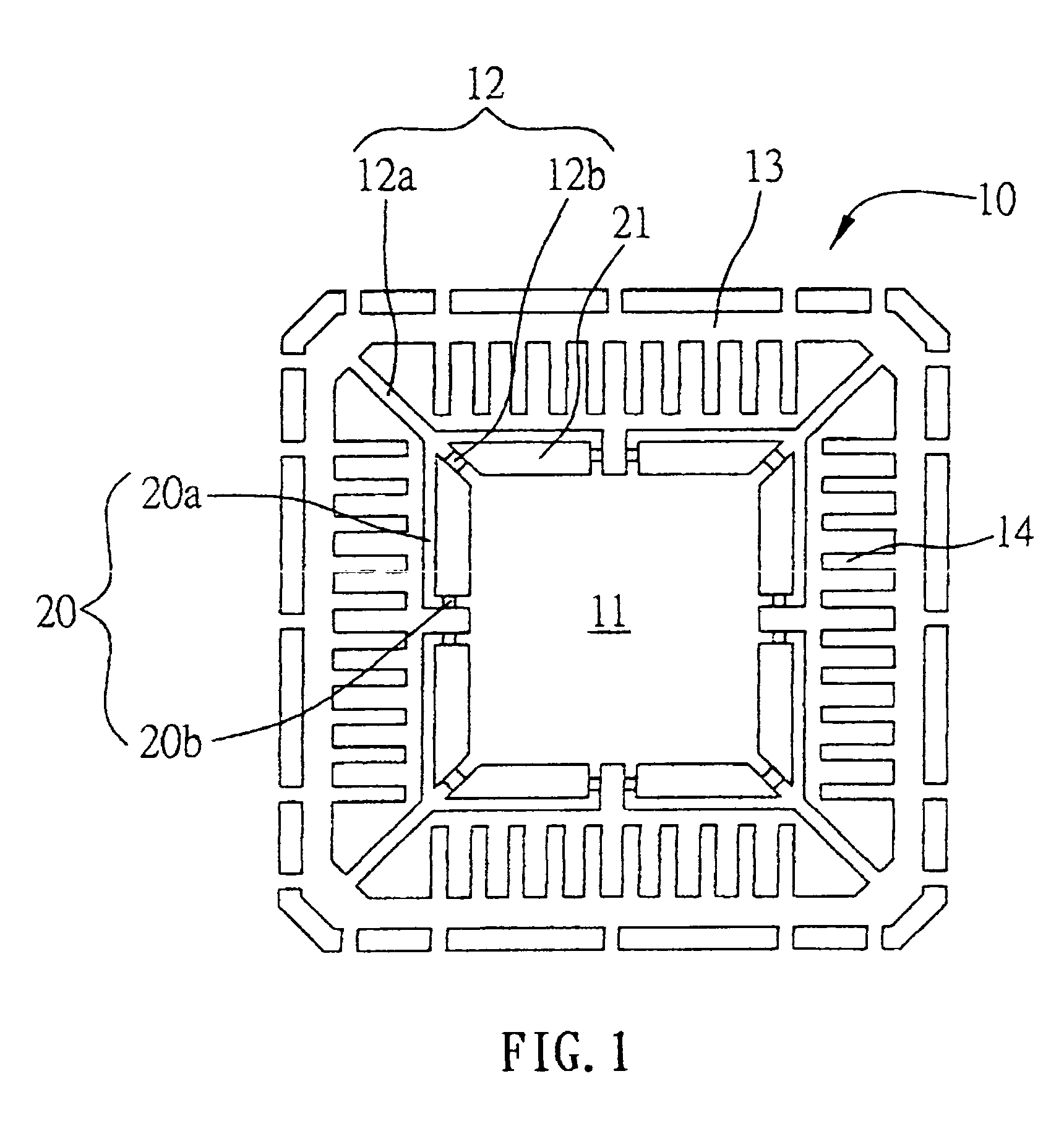
[0038]FIG. 4A shows a lead frame 10 according to the invention. As shown, this lead frame 10 is mostly the same in structure as that shown in FIG. 2 but differs in that, in addition to the first ground portions 20, at least one second ground portion 25 is formed and connected to each side edge 11a of the die pad 11, wherein the second ground portions 25 are not interconnected and not connected to the first ground portions 20. The second ground portion 25 comprises two connection areas 25b connected to the corresponding side edge 11a of the die pad 11, and a ground area 25a connected to the two connection areas 25b, such that the ground area 25a, the two connection areas 25b and the corresponding side edge 11a of the die pad 11 encompass to form a square hollow-out area 26. Similarly, the ground area 25a of the second ground portion 25 is coplanar with the leads 14, and the connection areas 25b are tilted to be accommodated to the height difference between the die pad 11 and the lead...

third embodiment

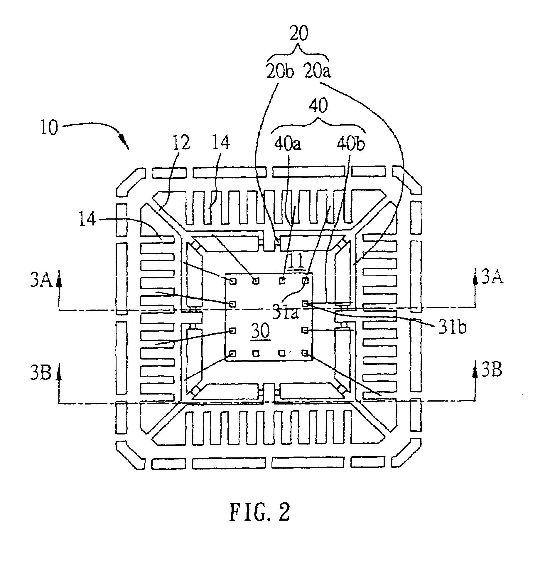
[0039]FIG. 4B shows a lead frame 10 according to the invention. As shown, this lead frame 10 differs from that shown in FIG. 2 in the design of the first ground portions 20. In this embodiment, there is no connection area 20b (FIG. 2) formed for the first ground portions 20 which thereby are suspended and not connected to the die pad 11, while the ground areas 20a of the first ground portions 20 remain coplanar with the leads 14. As a result, the bond pads 31b on the chip 30 can be directly electrically connected to the horizontal ground areas 20a via the ground wires 40b. During a high-temperature process, the horizontal ground areas 20a of the first ground portions 20 according to this embodiment are provided with even larger space for accommodating the thermal expansion thereof and releasing the thermal stresses, such that deformation of the first ground portions 20 can be prevented without affecting the grounding performance.

[0040]In a fourth embodiment of the invention as shown...


PUM


Abstract

A ground-enhanced semiconductor package and a lead frame used in the package are provided. The semiconductor package includes a lead frame having a die pad, a plurality of tie bars connected with and supporting the die pad, a plurality of leads surrounding the die pad, and a ground structure, wherein the ground structure comprises at least one of first ground portions connected to the tie bars, and / or at least one of second ground portions connected to the die pad, and wherein the first ground portions are separate from each other, and the second ground portions are separate from each other; at least one chip mounted on the die pad and electrically connected to the leads and the ground structure; and an encapsulation body for encapsulating the chip and the lead frame. The separately-arranged ground portions allow thermal stresses to be released from the ground structure without rendering deformation issues.

Description

FIELD OF THE INVENTION [0001]The present invention relates to ground-enhanced semiconductor packages, and more particularly, to a lead-frame-based semiconductor package which can prevent thermal deformation of ground areas thereof to promote the electricity performance.BACKGROUND OF THE INVENTION [0002]A conventional semiconductor package, such as Quad Flat Package(QFP) or Quad Flat Non-leaded(QFN) package, uses a lead frame as a chip carrier having a die pad and a plurality of leads, allowing at least one chip to be mounted on the die pad and electrically connected to the leads by a plurality of bonding wires which are bonded to bond pads on a surface of the chip. An encapsulation body is adopted to encapsulate the chip, the lead frame, and the bonding wires to thereby form the semiconductor package. Moreover, the die pad can be made to have one surface thereof exposed to outside of the encapsulation body, and such an exposed-pad type package facilitates dissipation of heat from th...

Claims


Application Information

Patent Timeline
IPC IPC(8): H01L23/495H01L23/04H01L23/52
CPCH01L23/49503H01L23/49541H01L24/49H01L2224/48091H01L2224/48095H01L2224/48247H01L24/48H01L2924/01005H01L2924/01029H01L2924/01082H01L2224/32257H01L2224/48253H01L2924/01033H01L2224/49171H01L2924/00014H01L2924/00H01L2924/351H01L2924/181H01L2224/05554H01L2224/45099H01L2224/05599H01L2924/00012
Inventor LEE, YI-SHIUNGLI, CHUN-YUANCHEN, HOLMANHUANG, SHIH-TSUNYUN, CHIH-YUNG
Owner SILICONWARE PRECISION IND CO LTD
Why Eureka
Try Eureka