PCB capable of releasing thermal stress

a printed circuit board and thermal stress technology, applied in the direction of printed circuit stress/warp reduction, printed circuit aspects, electrical apparatus construction details, etc., can solve the problems of thermal expansion of pwb b>, pwb b>, > in dimensions becomes wors

Active Publication Date: 2007-05-29
HANNSTAR DISPLAY CORPORATION
View PDF5 Cites 12 Cited by
  • Summary
  • Abstract
  • Description
  • Claims
  • Application Information

AI Technical Summary

Benefits of technology

[0011]To achieve the objective, the present invention discloses a PCB capable of releasing thermal stress. The PCB comprises a slender substrate, a thermal compression area and at least a slit. The thermal compression area, placed on the slender substrate, has a plurality of bonding pads for a plurality of TCPs to be mounted thereon and a plurality of dummy pads placed between the TCPs. The slit transversely crosses the thermal compression area and slices some of the dummy pads. When the TCPs are connected to the bonding pads of the PCB, the thermal compression area is heated up around from 150° C. to 200° C. Therefore, the slit can block the thermal expansion to be accumulated along the longitudinal direction of the thermal compression area.

Problems solved by technology

Unfortunately, the problem of thermal expansion for the PWB 121 or the PWB 122 in dimensions becomes worse than an early one, even though the cost and weight are reduced.

Method used


Image

  • PCB capable of releasing thermal stress
  • PCB capable of releasing thermal stress
  • PCB capable of releasing thermal stress

Examples


Embodiment Construction

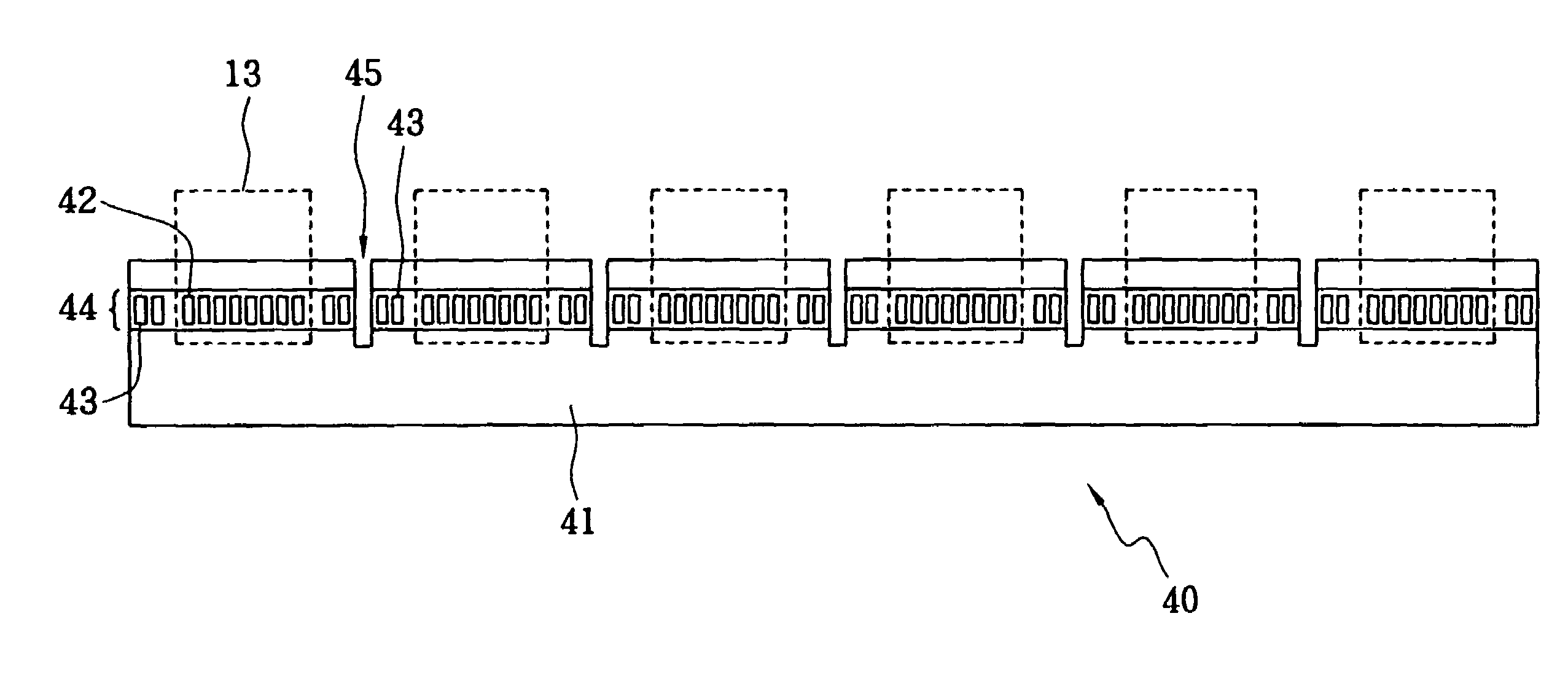
[0019]FIG. 3(a) is a schematic diagram of a PCB with a slit in accordance with the present invention. A PCB 30 comprises a slender substrate 31, a thermal compression area 34 and a slit 35. The thermal compression area 34, placed on the slender substrate 31, has a plurality of bonding pads 32 for the plurality of TCPs 13 to be mounted thereon and a plurality of dummy pads 33 placed between the TCPs 13. The slit 35 transversely crosses the thermal compression area 35 and slices some of the dummy pads 32. When the TCPs 13 are connected to the bonding pads 32 of the PCB 30, the thermal compression area 34 is heated to around 150° C. to 200° C. Therefore, the slit 35 can block the thermal expansion to be accumulated along the longitudinal direction of the thermal compression area 34. In comparison with the prior art in FIG. 1, the total elongation of the PCB 30 is half the total elongation of the PWB 121.

[0020]As shown in FIG. 3(b), the slit 35 is from the edge adjacent to the bonding p...


PUM


Abstract

A PCB comprises a slender substrate, a thermal compression area and at least a slit. The thermal compression area, placed on the slender substrate, has a plurality of bonding pads for a plurality of TCPs to be mounted thereon and a plurality of dummy pads placed between the TCPs. The slit transversely crosses the thermal compression area and slices some of the dummy pads. When the TCPs are connected to the bonding pads of the PCB, the thermal compression area is heated to around 150° C. to 200° C. Therefore, the slit can block the thermal expansion to be accumulated along the longitudinal direction of the thermal compression area.

Description

BACKGROUND OF THE INVENTION[0001]1. Field of the Invention[0002]The present invention relates to a PCB (printed circuit board) capable of releasing thermal stress, and more particularly, to a PCB or a PWB (printed wiring board) with slits for reducing thermal expansion.[0003]2. Description of the Related Art[0004]Recently, a liquid crystal display panel, a type of flat display, has been widely used as a display for PDAs, laptop computers, TVs, and so on.[0005]As shown in FIG. 1, in a liquid crystal display module adopting the aforesaid liquid crystal display panel, tapes 13 with drive IC chips 14 thereon are used in connecting a liquid crystal display panel 11 and the IC chips 14. Each of TCPs 15 (tape chip carriers), including an IC chip 14 and a tape 13, is connected to either a PWB (printed wiring board) 121 or a PWB 122.[0006]The structure of the PWB 121 gradually changed into a 4-layer board from an early 6-layer board due to reduction in cost. Similarly, the PWB 122 gradually ...

Claims


Application Information

Patent Timeline
Patent Type & Authority Patents(United States)
IPC IPC(8): H05K1/03
CPCH05K1/0271H05K1/117H05K1/142H05K1/147H05K3/3494H05K3/361H05K2201/09063H05K2201/09781H05K2203/0195
Inventor HO, SHU LINWANG, SHIH CHIEH
Owner HANNSTAR DISPLAY CORPORATION
Why Eureka
Try Eureka