
Backwards-compatible memory module

a memory module and backward compatibility technology, applied in the field of backward compatibility memory modules, can solve the problem that production capacity can only be used inefficiently

Inactive Publication Date: 2007-05-22
POLARIS INNOVATIONS LTD
View PDF5 Cites 8 Cited by
  • Summary
  • Abstract
  • Description
  • Claims
  • Application Information

AI Technical Summary

Benefits of technology

[0023]One major difference between DDR2 memory modules and DDR1 memory modules is the doubling of the number of prefetch registers and, at the same time, the doubling of the second clock signal, which controls the controlled switching device, in the changeover from DDR memory modules of the first generation (DDR1) to the second (DDR2). Thus, in the case of DDR2, the second clock signal will internally be at twice the clock frequency of the first clock signal, which clocks the read / write control device, thus resulting in twice the data rates at the data inputs / outputs and data pins of the corresponding chip, compared to DDR1.
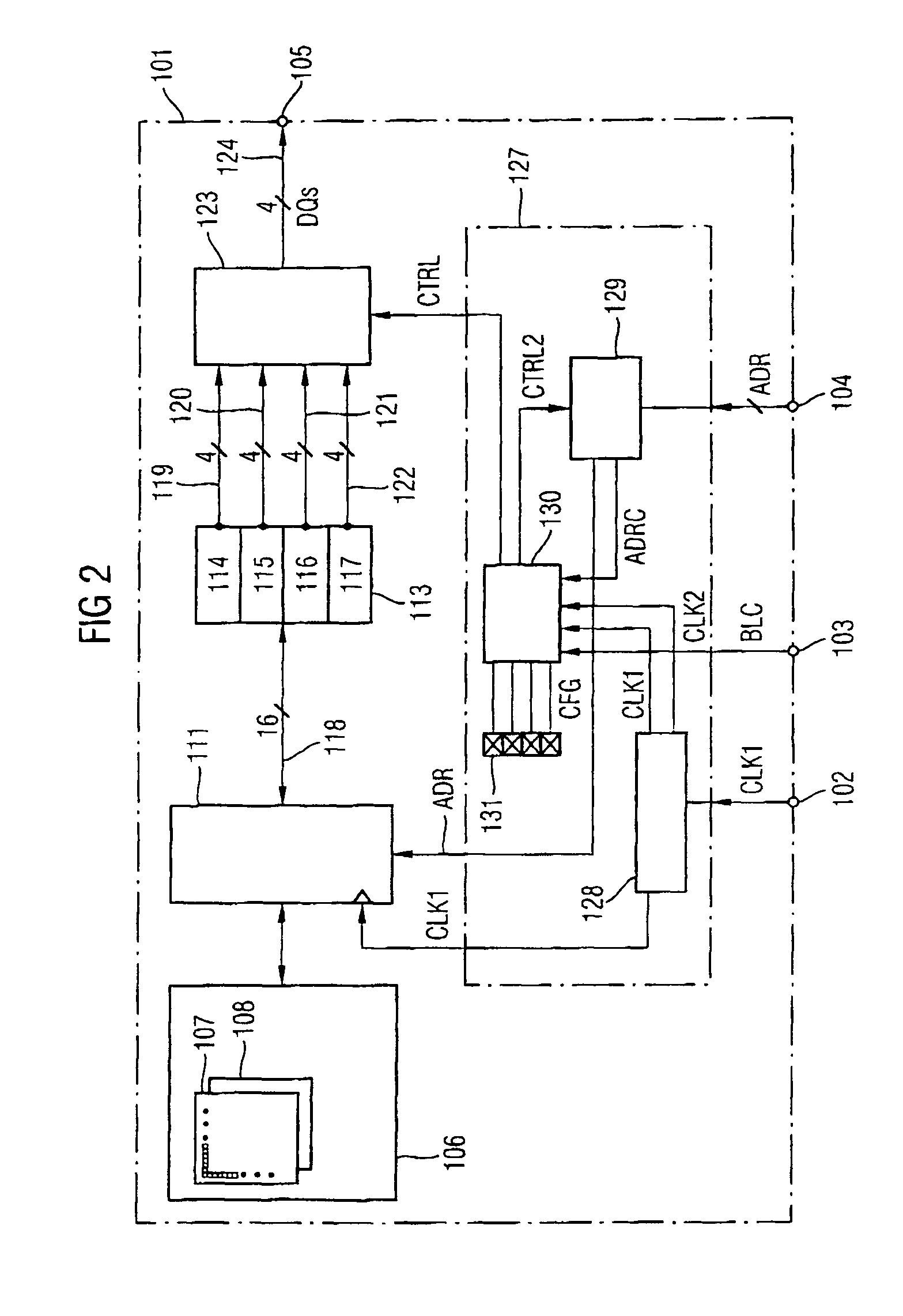
[0032]In one preferred embodiment, the control logic has at least one clock generator for production of a clock signal which is complementary to the first clock signal, and for production of the second clock signal. This has the advantage that a memory module according to the invention which is based on DDR2 SDRAM modules can be used in an appliance environment which is designed for SDR memory modules. Internally, the memory according to the invention produces a differential clock signal from the first clock signal and the complementary clock signal, because differential clock signals are generally used in DDR2 memory modules. This has the advantage that it is possible to use subelements from the DDR2 SDRAM production for the manufacture of a memory chip according to the invention.
[0038]In one preferred refinement of the memory module according to the invention, in the third operating mode, a read cycle is ended after half the number of prefetch registers have been coupled in a very short burst length. This has the advantage that a memory module according to the invention which is being operated in accordance with DDR2 requirements can be used as a DDR1 module in this third operating mode. In this case, only the first half of the prefetch registers which are provided are used. If the burst lengths are relatively long, this first half of the prefetch registers is then used repeatedly and successively for initial storage and outputting of memory data to the data inputs / outputs, until the appropriate number of data items have been produced at the data inputs / outputs, depending on the selected burst length.
[0041]Since more recent generation memory modules operate at lower supply voltages—for example 2.5 V is provided for DDR1 and 1.8 V or 1.5 V for DDR2 and DDR3—and since the memory module according to the invention is intended to receive both supply voltages for the older generations, for example SDR, around 3.3 V, this voltage regulation according to the invention allows better compatibility with different generations of memory modules.
[0044]One of the signal-ended control signals is preferably a data strobe signal. Since, for example, differential control signals are passed to the memory module in the DDR2 generations of memory modules, and that single-ended control signals are passed to them for older generations, the signal converter according to the invention is used to improve the compatibility with different generations of memory modules.

Problems solved by technology

This means that production capacities can be used only inefficiently, since the demand for older generations of memory modules generally decreases over time.

Method used


Image

  • Backwards-compatible memory module
  • Backwards-compatible memory module
  • Backwards-compatible memory module

Examples


Embodiment Construction

[0056]Identical and functionally identical elements are provided with the same reference symbols in the figures.

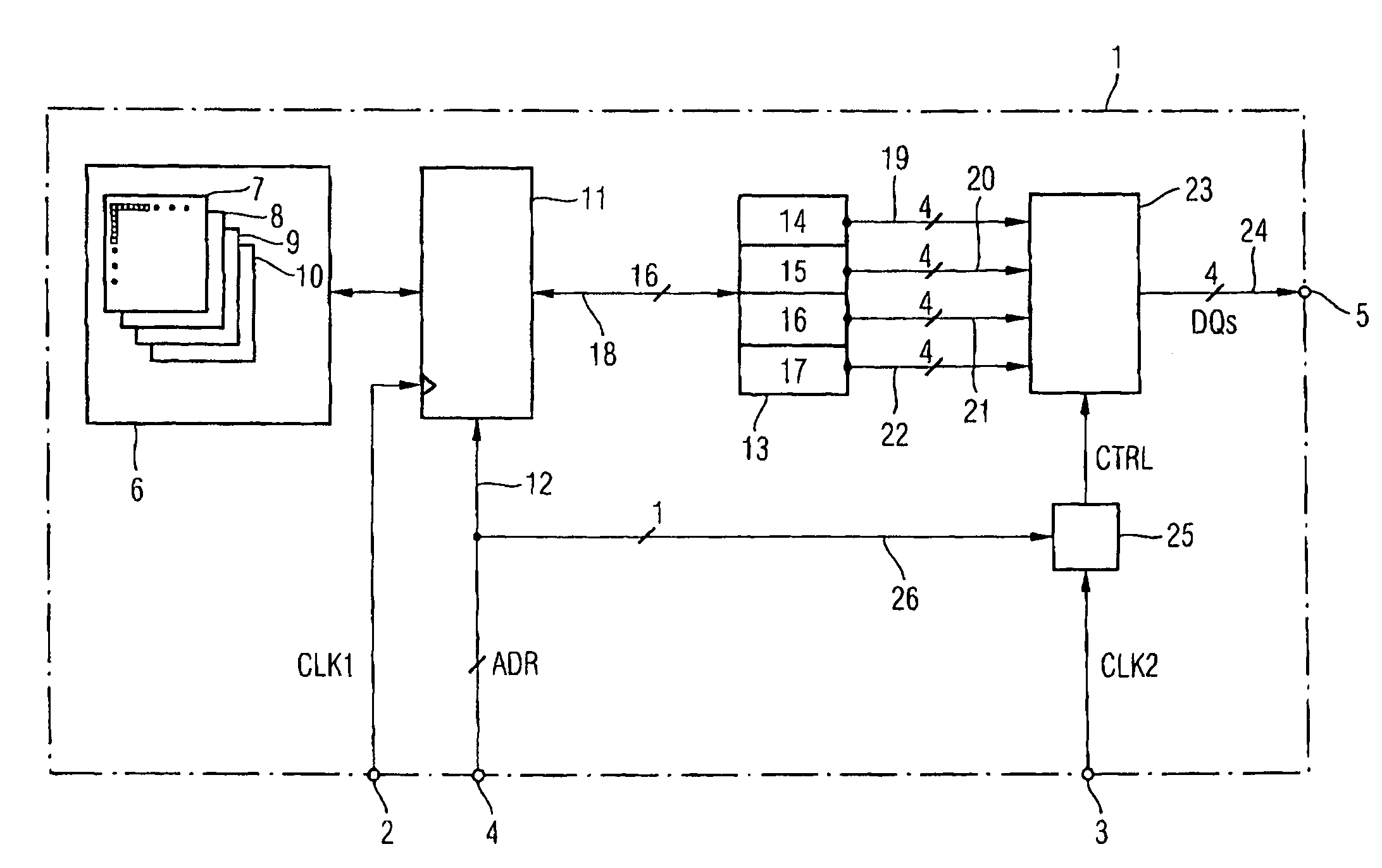
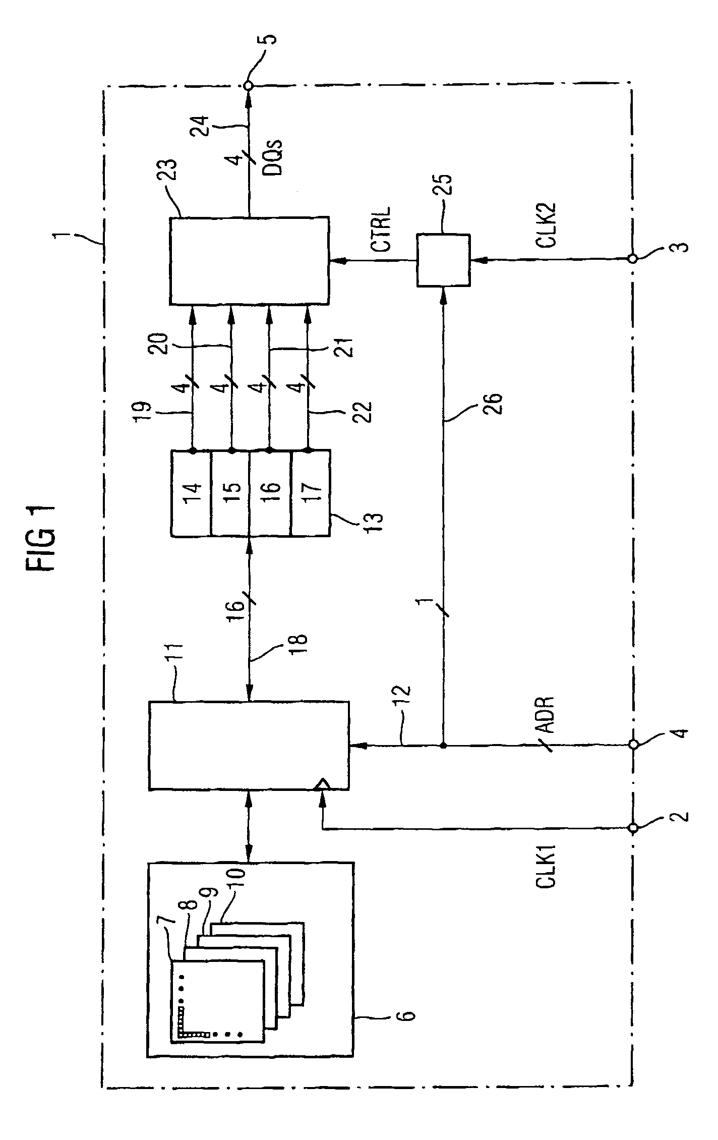
[0057]FIG. 1 shows a block diagram of the memory module 1 according to the invention.

[0058]The memory module 1 has a first clock input 2 for the first clock signal CLK1, a second clock input 3 for the second clock signal CLK2, address inputs 4 for address signals ADR, and data inputs / outputs 5 for memory data DQs.

[0059]The memory module 1 according to the invention has a memory cell array 6, which in this case has four memory banks 7, 8, 9, 10 with memory cells, with the corresponding memory cells in this exemplary embodiment being organized in an organization based on groups of four. This means that four memory cells are addressed at the same time by one address. Four bits are thus activated, starting from one initial address.

[0060]A clocked read / write control device 11 is provided, which is coupled to the first clock input 2 and is clocked by the first clock signal CLK1....


PUM


Abstract

A backwards-compatible memory module is disclosed. According to one aspect, a memory module comprises addressable memory cells organized in organization units having a predetermined number of memory cells, a read / write control device clocked by a first clock signal, a plurality of prefetch registers for initially storing data read from the memory cells wherein the register size corresponds to the predetermined number. In a first operating mode, a switching device clocked by a second clock signal successively couples the prefetch registers to data input / output terminals. The number of data input / output terminals corresponds to the predetermined number. In a second operating mode, the switching device is controlled by at least one address signal and couples at least one of the prefetch registers to the data input / output terminals.

Description

TECHNICAL FIELD[0001]The present invention relates to a backwards-compatible memory module, in particular for use as an SDR, DDR1, DDR2 and / or DDR3 SDRAM module.BACKGROUND ART[0002]The increasing speed of computer processors requires, in a corresponding manner, a higher speed for memory accesses and faster memory modules, in particular for RAMs (random access memories).[0003]Thus, in the past, various generations of RAMs have been developed whose access rate has risen continuously. The important factor is in each case to shorten the time intervals with which new data to be read from or written to the memory cell array is produced at the data inputs / outputs of the corresponding memory module. Starting from synchronous dynamic RAMs (SDRAM), so-called DDR SDRAMs have been developed, with twice the data rate (DDR=double data rate). More recently, the International JEDEC Standardization organization has proposed requirements for more recent generations of DDR2 and DDR3 SDRAMs.[0004]Since...

Claims


Application Information

Patent Timeline
Patent Type & Authority Patents(United States)
IPC IPC(8): G11C8/00G11C5/00G11C7/10G11C7/22G11C11/4093G11C11/4096
CPCG11C7/1045G11C7/1051G11C7/1066G11C7/1072G11C7/1078G11C7/22G11C11/4096G11C2207/107
Inventor FLACH, BJORNDE CASTRO MARTINS, MONICARUF, WOLFGANGSCHNELL, MARTIN
Owner POLARIS INNOVATIONS LTD
Learn More