Electro-optical device

a liquid crystal display and optical technology, applied in optics, identification means, instruments, etc., can solve the problems of reducing the aperture ratio, the gate bus line has not been able to provide a sufficient capacity by itself, and the pixel electrode portion is too small to store necessary electrical charge for a sufficient period of time, etc., to achieve stable operation, improve the effect of shading and advantageous transistor operation

Inactive Publication Date: 2007-04-17
SEMICON ENERGY LAB CO LTD
View PDF116 Cites 4 Cited by
  • Summary
  • Abstract
  • Description
  • Claims
  • Application Information

AI Technical Summary

Benefits of technology

[0017]Specifically, the common electrode is disposed such that it covers the bus lines, and the pixel electrode is disposed such that it overlaps the bus lines. Thus, the common electrode and the pixel electrode overlap each other, and this overlap provides an auxiliary capacitor. In addition, while at least one of the electrodes of a conventional auxiliary capacitor has been formed of an opaque material, both of such electrodes are formed of a transparent material according to the present invention. Thus, they will not hinder display and the aperture ratio is maintained.
[0021]When a top-gate type transistor (a transistor having a structure in which the gate electrode is provided on top of a semiconductor layer) is used as a switching transistor, it will be advantageous for stable operation of the transistor if light is allowed to be incident upon the substrate primarily from above, i.e., from the side of the pixel electrodes because this prevents light from entering the semiconductor layer under the gate electrode.
[0022]The effect of shading can be further improved for more stable operation by providing a film made of the same material as the layer of the source bus lines on top of the gate bus lines where the semiconductor layer and the gate bus lines intersect with each other.
[0024]Especially, a flat insulation layer formed by means of spin coating or the like will be effective in reducing surface irregularity for improved uniformity of an electric field applied to liquid crystal molecules.

Problems solved by technology

In an actual operation, however, the capacity of the pixel electrode portion is too small to store necessary electrical charge for a sufficient period of time by itself.
Although a capacitor formed using a gate bus line has been sufficient when the area of the pixel is large enough, a gate bus line has been unsuccessful in providing a sufficient capacity by itself when the area of the pixel is small.
Such a structure results in a decrease in the aperture ratio because a pixel includes an area where light is blocked.

Method used


Image

  • Electro-optical device
  • Electro-optical device
  • Electro-optical device

Examples


first embodiment

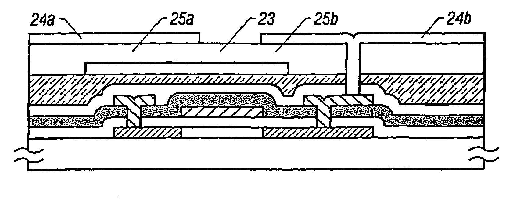
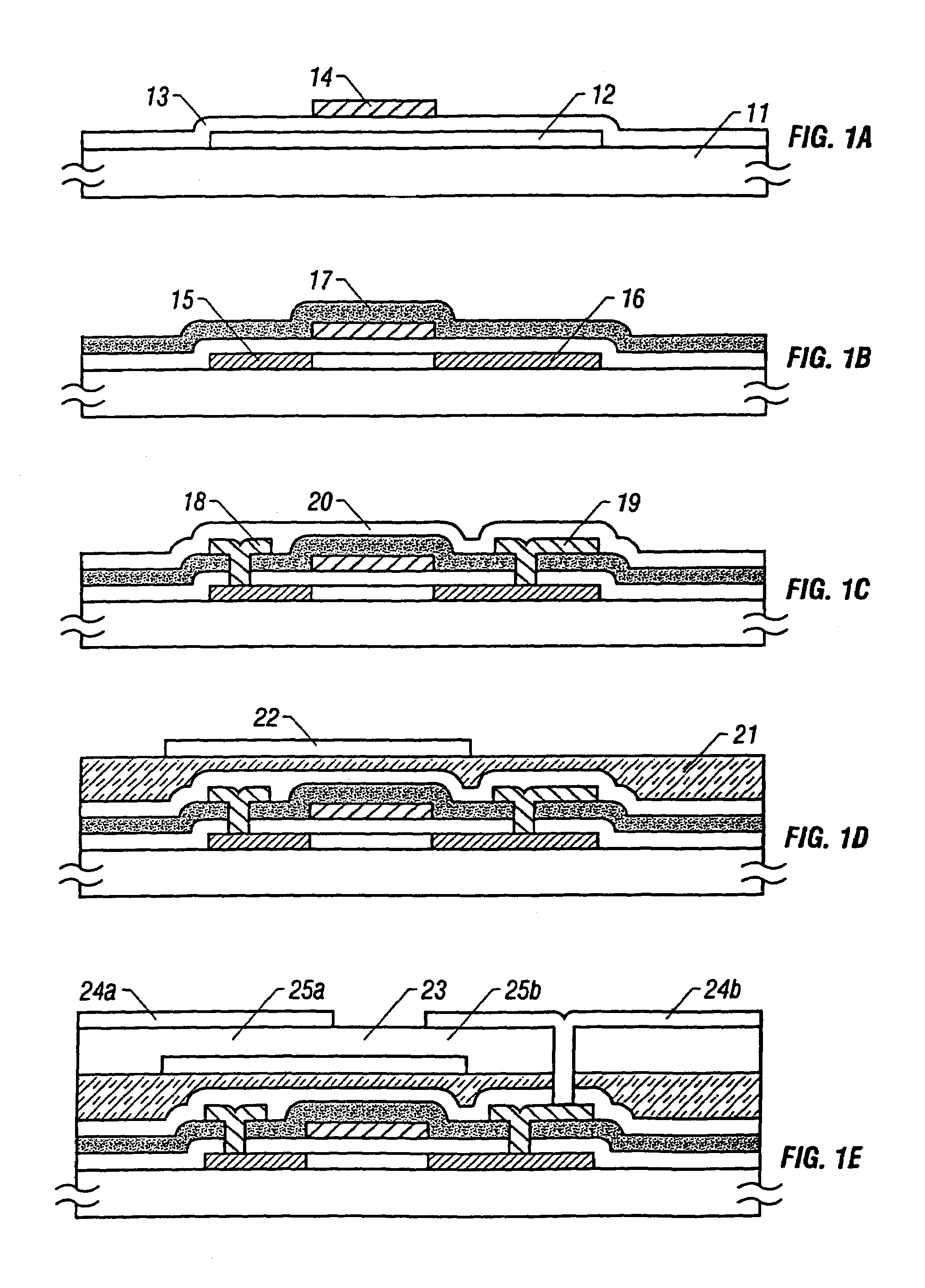
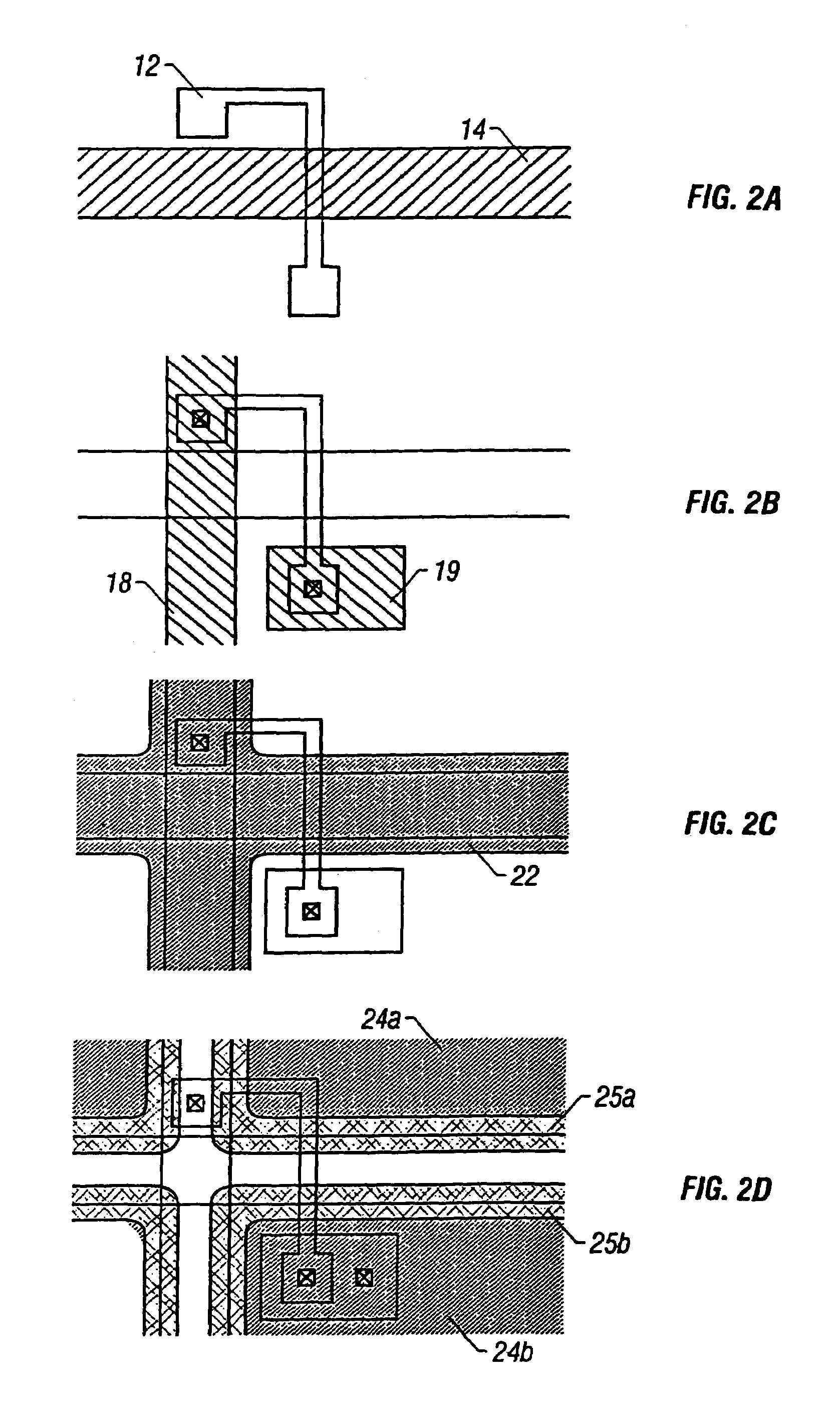
[0030]the present invention will now be described. FIGS. 1A through 1E and FIGS. 2A through 2D show a configuration of a pixel of an active matrix type liquid crystal display which employs the invention disclosed in this specification. FIGS. 1A through 1E are schematic sectional views showing fabrication steps according to the present embodiment, and FIGS. 2A through 2D show the configuration of each of a bus line, a common electrode, pixel electrodes, a semiconductor layer, and the like according to the present embodiment. The reference numbers in FIGS. 2A through 2D are in correspondence with those in FIGS. 1A through 1E. FIGS. 1A through 1E are conceptual views and are not exactly identical to FIGS. 2A through 2D in configuration.

[0031]Further, FIGS. 1A through 1E and FIGS. 2A though 2D show a configuration of only a substrate on which a thin film transistor is provided. In practice, there is provided another substrate opposite thereto (opposite substrate), and liquid crystal is ...

second embodiment

[0045]the present invention will now be described. FIGS. 3A through 3E and FIGS. 4A through 4D show a configuration of a pixel of an active matrix type liquid crystal display which employs the invention disclosed in this specification. FIGS. 3A through 3E are schematic sectional views showing fabrication steps according to the present embodiment, and FIGS. 4A through 4D show the configuration of each of a bus line, a common electrode, pixel electrodes, a semiconductor layer, and the like according to the present embodiment. The reference numbers in FIGS. 4A through 4D are in correspondence with those in FIGS. 3A through 3E. FIGS. 3A through 3E are conceptual views and are not exactly identical to FIGS. 4A through 4D in configuration.

[0046]As shown in FIG. 3A, a semiconductor layer (active layer) 32 of a transistor is provided on a glass substrate 31 having an underlying silicon oxide film (not shown). A gate insulation film 33 is formed so as to cover the active layer 32. A gate bus...


PUM


Abstract

An auxiliary capacitor for a pixel of an active matrix type liquid crystal display is provided without decreasing the aperture ratio. A transparent conductive film for a common electrode is formed under a pixel electrode constituted by a transparent conductive film with an insulation film provided there between. Further, the transparent conductive film for the common electrode is maintained at fixed potential, formed so as to cover a gate bus line and a source bus line, and configured such that signals on each bus line are not applied to the pixel electrode. The pixel electrode is disposed so that all edges thereof overlap the gate bus line and source bus line. As a result, each of the bus lines serves as a black matrix. Further, the pixel electrode overlaps the transparent conductive film for the common electrode to form a storage capacitor.

Description

CROSS-REFERENCE TO RELATED APPLICATIONS[0001]This application is a divisional application of U.S. application Ser. No. 10 / 267,526, filed Oct. 8, 2002, now U.S. Pat. No. 6,914,260, which is a continuation of U.S. Ser. No. 09 / 850,886, filed May 7, 2001, now U.S. Pat. No. 6,475,837, which is a continuation of U.S. Ser. No. 09 / 360,841, filed Jul. 22, 1999, now U.S. Pat. No. 6,246,453, which is a continuation of U.S. Ser. No. 08 / 881,182, filed on Jun. 24, 1997, now U.S. Pat. No. 5,982,460, which claims the benefit of a foreign priority application filed in Japan as Ser. No. 08-185638 on Jun. 25, 1996. This application claims priority to each of these prior applications, and the disclosures of the prior applications are considered part of and are incorporated by reference in the disclosure of this application.BACKGROUND OF THE INVENTION[0002]1. Field of the Invention[0003]The invention disclosed in this specification relates to a configuration of a pixel region of an active matrix type li...

Claims


Application Information

Patent Timeline
Patent Type & Authority Patents(United States)
IPC IPC(8): G02F1/1343G02B5/00G02F1/136G02F1/1362G02F1/1368G09F9/00H01L29/786
CPCG02F1/136209G02F1/136213G02F1/136286G02F1/136227G02F2201/121G02F2201/40
Inventor ZHANG, HONGYONGYAMAGUCHI, NAOAKITAKEMURA, YASUHIKO
Owner SEMICON ENERGY LAB CO LTD
Why Eureka
Try Eureka