
High speed data bit latch circuit

a latch circuit and data bit technology, applied in the direction of instruments, computation using denominational number representation, pulse technique, etc., can solve the problems of constant facet of high-speed data busses, unbalanced combination of speed without memory density, and cpu alone cannot increase computer performance, etc., to achieve minimal hold time, no setup time, and reliable latch

Inactive Publication Date: 2007-03-20
URENSCHI ASSETAB LIABILITY
View PDF2 Cites 2 Cited by
  • Summary
  • Abstract
  • Description
  • Claims
  • Application Information

AI Technical Summary

Benefits of technology

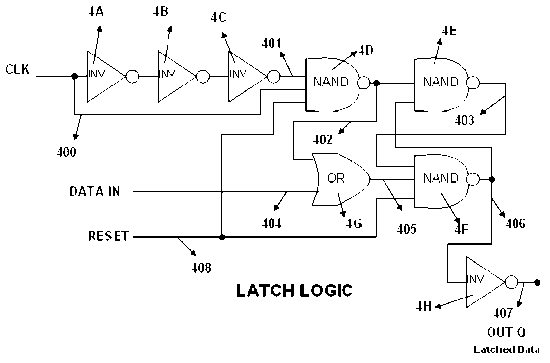
[0019]It is an object of this invention to provide a latching circuit which requires no setup time and a minimal hold time, and still latches reliably.

Problems solved by technology

The computer industry, with the advances of silicon technology, is constantly faced with the complexities of high speed data busses.
However, speed without density of memory is an unbalanced combination.
The CPU by itself cannot increase computer performance without a high speed memory sub-system and without such a high speed memory the CPU does not perform at the speed it was designed for.
When memory access is substantially slower than CPU speed a bottleneck is created between memory and CPU Front End bus.
(a) Data bus widths must be broad enough to satisfy wide data bus requirements of the modern CPU.
(b) High Memory density must be maintained on the same data bus. That is, more Memory Modules are attached to the same data bus, and more connectors appear on the motherboard attached to the bus.
(c) The presence of parasitic resistors, inductors and capacitors (RLC) in the structure of the data bus and on the devices, including connectors, memory modules, printed circuit boards, memory chips and logic chips connected to the bus must be overcome.
(d) Effects of the physical RLC quantities affecting the overall speed by which data can be transported on the bus and thus affecting the overall performance and bandwidth of such bus.
(e) Synchronization of the Data signals and Strobe signals required to latch the data at the destination receiver.
However, further increases in computer speed have created synchronization and data capturing problems in the reading and writing of data between the system bus and the memory banks either directly or indirectly, as described in said prior art.

Method used


Image

  • High speed data bit latch circuit
  • High speed data bit latch circuit
  • High speed data bit latch circuit

Examples


Embodiment Construction

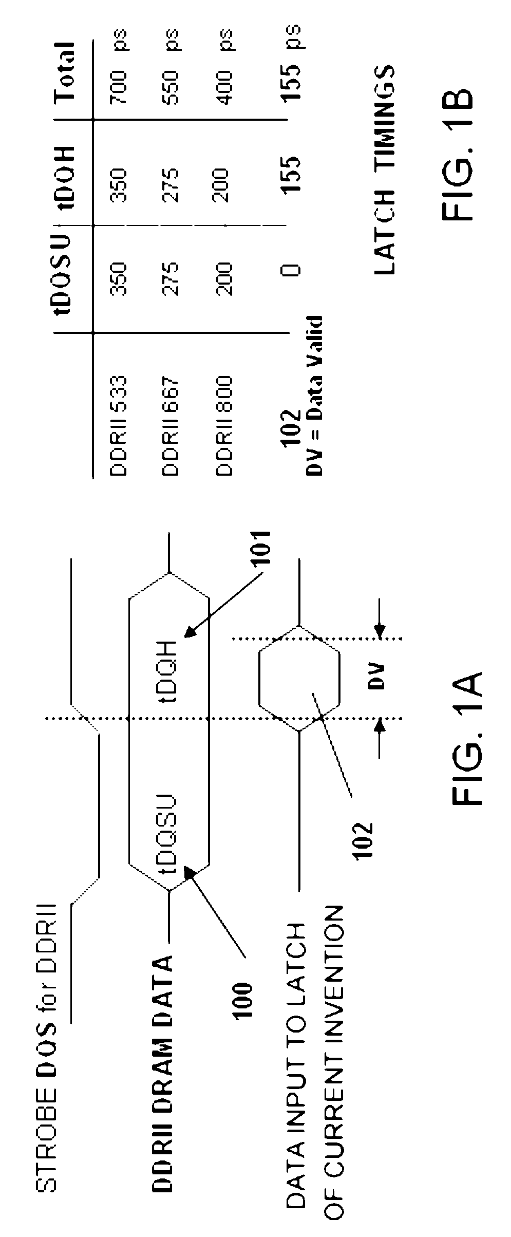
[0037]For this disclosure it is assumed that the data is latched into the latching element with the transition of the clock edge from Low to High level. The data must be presented to the data input of the latch within a specified minimum time after the rising edge of the applied clock to the latch and it must also stay active for a specified minimum time after the rising edge of the clock.

[0038]Once these times are satisfied, the value of data at the input will be preserved at the output of the latch until the next rising edge of the clock when the new data input value will be sampled and stored into the latch to be preserved until the following rising clock edge. After the specified DATA hold times, the data could change value at the input of the latch without affecting the latched data value at the output. The output of the latch will only change with the rising edge of the clock and the data value as specified.

[0039]In implementations of the prior art, the clock and the data reac...


PUM


Abstract

A latching circuit having a clock signal input and a data input, includes an inverting delay circuit having an input connected to DATA IN and having an output signal s1, a NAND circuit having a first input connected to signal s1, a second input connected to the clock signal, and an output signal s2, an OR circuit having a first input connected to the data input, a second input connected to s2, and an output signal s3, and a FLIP-FLOP circuit whose first input is connected to s2, whose second input connected to s3, and whose output is OUT Q.

Description

BACKGROUND OF INVENTION[0001]The computer industry, with the advances of silicon technology, is constantly faced with the complexities of high speed data busses. The high speed of microprocessor CPUs requires a high speed data bus between the memory subsystem and the front end CPU data bus. However, speed without density of memory is an unbalanced combination. Modern computer systems require increasingly large RAM arrays, and these arrays are packaged in modules of approximately the same size as used in previous, lower capacity memories. Thus, the density of the memory modules, in bits or bytes per square inch of circuit board, is constantly increasing.[0002]The CPU by itself cannot increase computer performance without a high speed memory sub-system and without such a high speed memory the CPU does not perform at the speed it was designed for. When memory access is substantially slower than CPU speed a bottleneck is created between memory and CPU Front End bus. With advances of the...

Claims


Application Information

Patent Timeline
Patent Type & Authority Patents(United States)
IPC IPC(8): H03K19/00
CPCH03K3/037
Inventor KARABATSOS, CHRIS
Owner URENSCHI ASSETAB LIABILITY
Learn More