
Optical element module package and method for manufacturing the same

a technology of optical elements and modules, applied in the direction of optical waveguide light guides, semiconductor laser structural details, semiconductor lasers, etc., can solve the problems of increasing manufacturing costs, inconvenient manufacturing procedures, and unsuitable optical element packages for high-speed transmission above several gbps, and achieves simple, reliable and inexpensive implementation.

Inactive Publication Date: 2007-01-02
SAMSUNG ELECTRONICS CO LTD
View PDF14 Cites 7 Cited by
  • Summary
  • Abstract
  • Description
  • Claims
  • Application Information

AI Technical Summary

Benefits of technology

[0011]Accordingly, the present invention has been made to overcome the above-mentioned problems and to provide additional advantages, by introducing a package applicable to a fast, large-capacitance optical element module owing to its excellent radio-frequency characteristics and a method for manufacturing the same.
[0012]One aspect is that the present invention may be realized in a simple, reliable, and inexpensive implementation.

Problems solved by technology

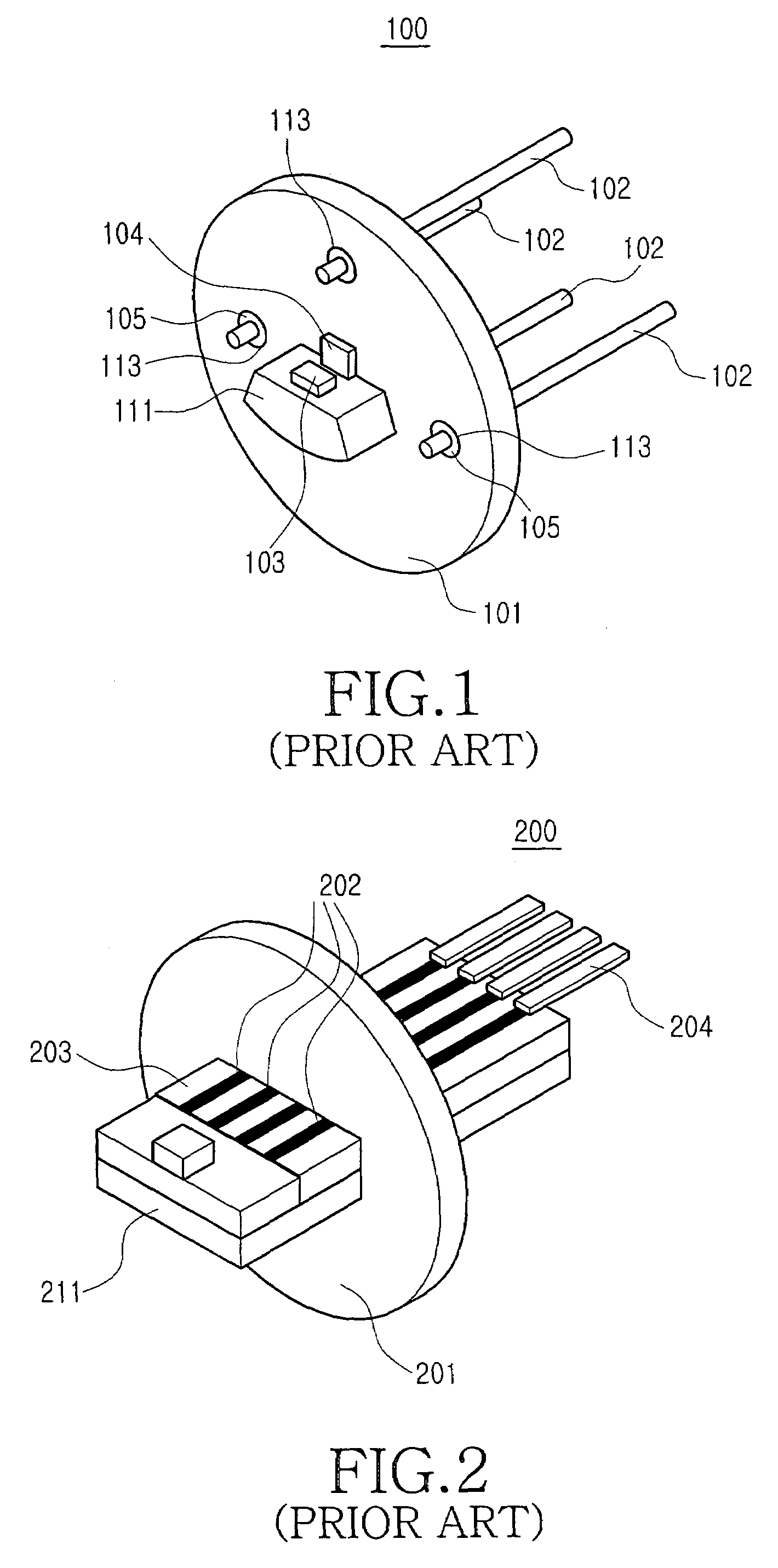
However, this type of optical element package is not suitable for a high-speed transmission above several Gbps because the package may suffer from an inherent inductance of its leads, a parasitic capacitance between its leads and stem, and a characteristic impedance mismatch that may occur while radio-frequency signals inputted from outside pass through the respective leads.
Moreover, the manufacturing procedure is inconvenient as the respective leads must be aligned with a plurality of through-holes in the stem and the though-holes must be sealed individually.
First, the feedthrough 203, having a ceramic-laminated structure, is formed through a low temperature co-fired ceramic (LTCC) process at the temperature up to 800–1000° C. Such a high temperature process increases the manufacturing cost.
In addition, it is difficult to guarantee a hermeticity between the feedthrough 203 and the stem 201.
All these factors leads to an unreliable product.

Method used


Image

  • Optical element module package and method for manufacturing the same
  • Optical element module package and method for manufacturing the same
  • Optical element module package and method for manufacturing the same

Examples


Embodiment Construction

[0024]Hereinafter, an optical element module package and a method for manufacturing the same according to preferred embodiments of the present invention will be described with reference to the accompanying drawings. For the purposes of clarity and simplicity, a detailed description of known functions and configurations incorporated herein will be omitted as it may make the subject matter of the present invention unclear.

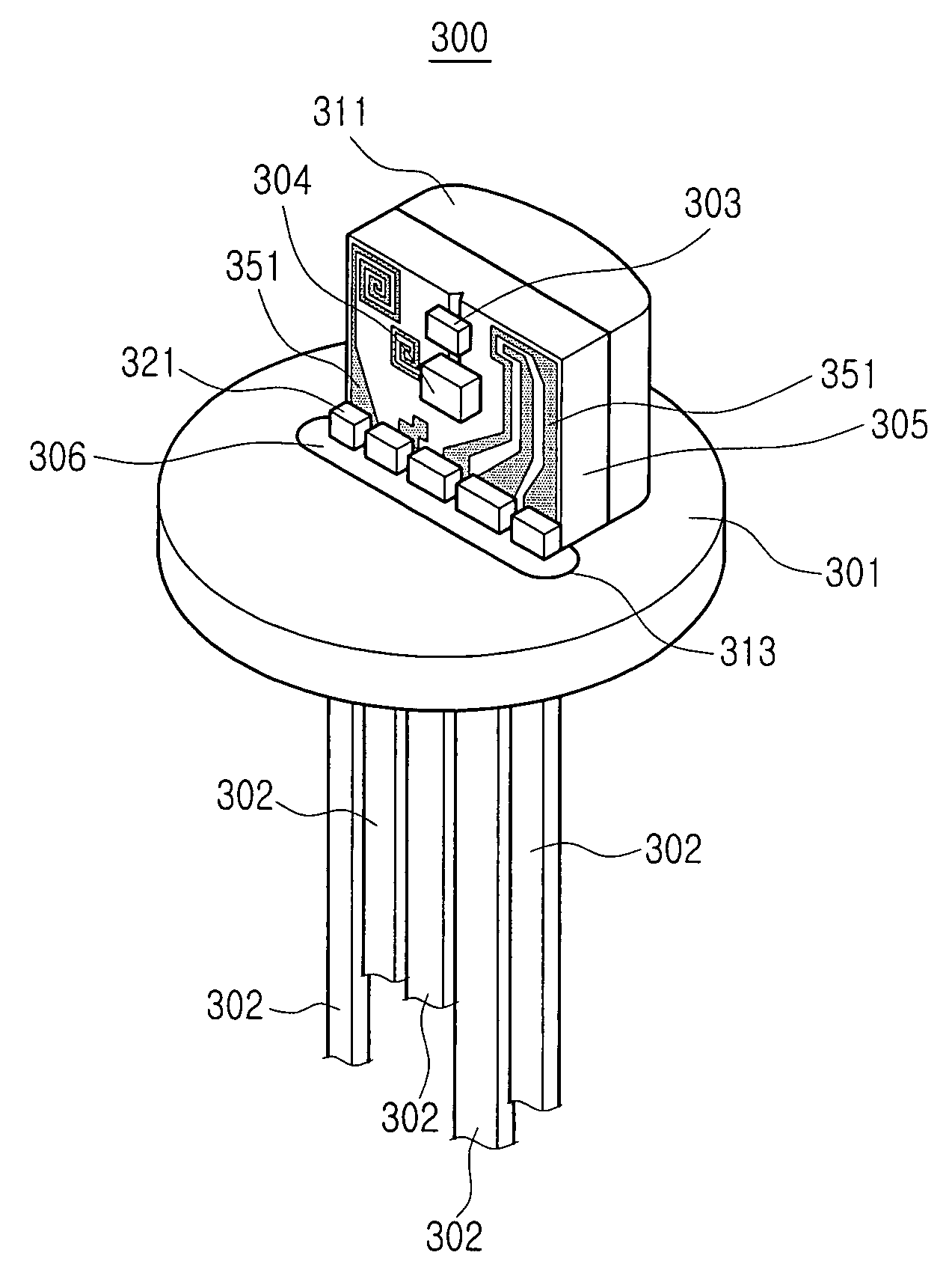
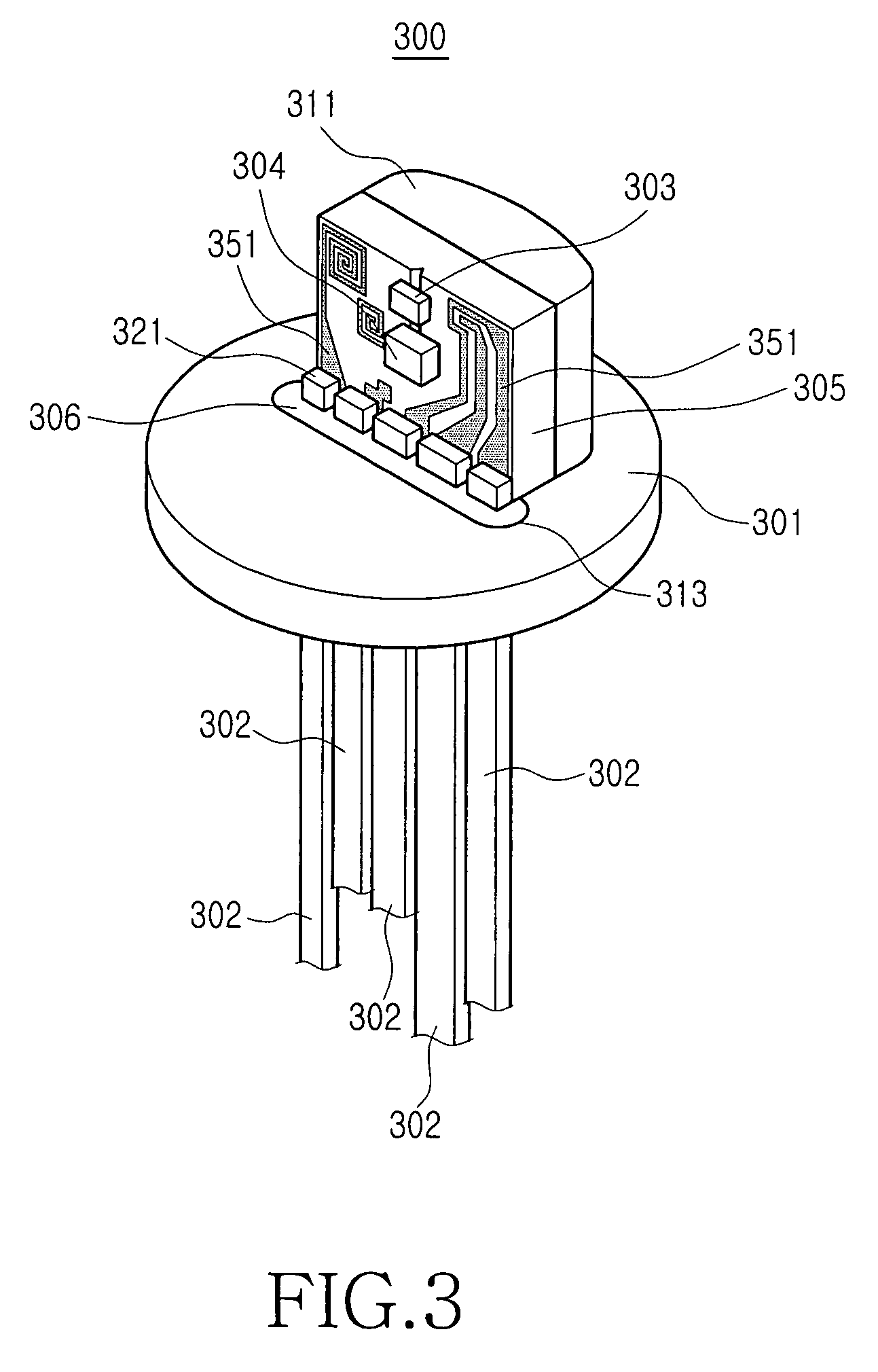
[0025]As shown in FIGS. 3 to 5, an optical element module package 300 according to a first preferred embodiment of the present invention includes a stem 301 having a heat sink block 311 formed at one end thereof, a sub-mount 305 having a laser diode 303 and a photo diode 304 mounted thereon, and a plurality of leads 302 formed at the other end. In operation, the package 300 projects optical signals when radio-frequency signals are applied to the laser diode 303 and the photo diode 304 mounted on the sub-mount 305.

[0026]The stem 301 has an elongated through-hole 313 e...


PUM


Abstract

An optical element module package with a TO-can structure is disclosed. The module includes a laser diode for projecting optical signals and a photo diode for monitoring the optical signals projected from the laser diode. The package includes a stem having a first through-hole formed in a long-hole shape parallel to the diametrical direction of the stem, the first through-hole extending through the stem from one side to the other; and a plurality of leads arranged in a row through the first through-hole. The first through-hole is filled with a sealant of a glass material so that the stem and the leads are fixed.

Description

CLAIM OF PRIORITY[0001]This application claims priority to an application entitled “optical element module package and method for manufacturing the same,” filed with the Korean Intellectual Property Office on Jun. 4, 2003 and assigned Serial No. 2003-35965, the contents of which are hereby incorporated by reference.BACKGROUND OF THE INVENTION[0002]1. Field of the Invention[0003]The present invention relates to an optical element module, and more particularly to an optical element module package having a TO-can structure and a method for manufacturing the same.[0004]2. Description of the Related Art[0005]In general, an optical element module, mounted on an electric circuit device (e.g., a printed circuit board), modulates radio-frequency signals into optical signals. Due to a rapid development in the information industry, there is an increasing trend to transmit information by means of an optical communication network as a result of faster and larger data capacity demands. Traditiona...

Claims


Application Information

Patent Timeline
Patent Type & Authority Patents(United States)
IPC IPC(8): H01S3/04G02B6/42G02B6/12H01S5/00H01S5/02H01S5/0231H01S5/0232H01S5/024H01S5/0683
CPCH01S5/02212H01S5/0683H01S5/02248H01S5/02244H01S5/0231H01S5/02325H01S5/0232G02B6/42
Inventor KEH, YONG-CHANPARK, MUN-KUE
Owner SAMSUNG ELECTRONICS CO LTD
Learn More