
Method and apparatus for calibrating a delay line

a delay line and calibration method technology, applied in the field of semiconductor integrated circuits, can solve the problems of reducing the efficiency of the calibration circuit, affecting the timing of the design, and the possibility of overshooting the desired delay line setting, so as to reduce the difference, reduce the difference, and reduce the difference

Inactive Publication Date: 2007-01-02
AVAGO TECH INT SALES PTE LTD
View PDF10 Cites 32 Cited by
  • Summary
  • Abstract
  • Description
  • Claims
  • Application Information

AI Technical Summary

Benefits of technology

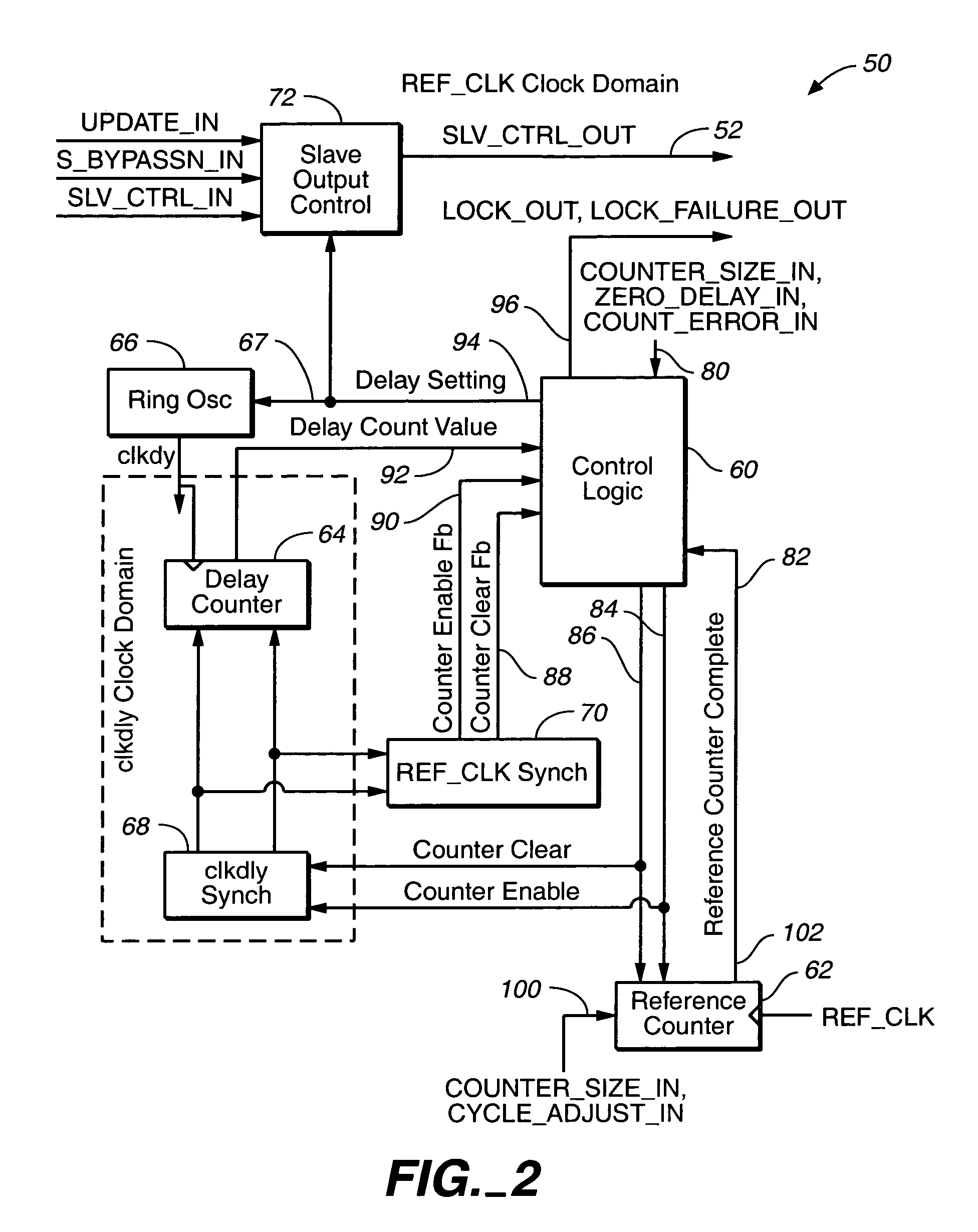
The present invention provides a delay line calibration circuit and a data capture circuit that can calibrate the delay of a programmable delay line to a reference clock. The circuit includes a master delay line, delay counter, reference counter, and control circuit. The control circuit compares the delay count to the reference count and generates a modified value for the delay setting to reduce the difference between the two. This allows for precise control of the delay through the programmable delay line. The data capture circuit includes a reference clock, data input, and strobe input, which can capture data based on a delayed strobe signal. The delay line has a propagation delay that is a function of the delay setting, and the circuit includes a delay counter and reference counter to accurately measure this delay. The technical effects of this invention include improved precision and accuracy in delay control and data capture.

Problems solved by technology

If a large number of iterations is required, this can adversely affect the efficiency of the calibration circuit.
Another disadvantage of a binary search algorithm and potentially other algorithms is that it is possible to overshoot the desired delay line setting.
If the slave delay line in the calibration circuit is used within a ring oscillator, overshooting the delay line setting can temporarily create a very high frequency system that makes meeting design timing difficult.
In addition, multiple delay cells are required, thus adding area to the design.
A further disadvantage is that a fixed number of delay cells causes the single cell delay value to be a fixed fractional value of the reference clock, thus making the circuit unable to lock on to other fractional values of the reference clock.

Method used


Image

  • Method and apparatus for calibrating a delay line
  • Method and apparatus for calibrating a delay line
  • Method and apparatus for calibrating a delay line

Examples


Embodiment Construction

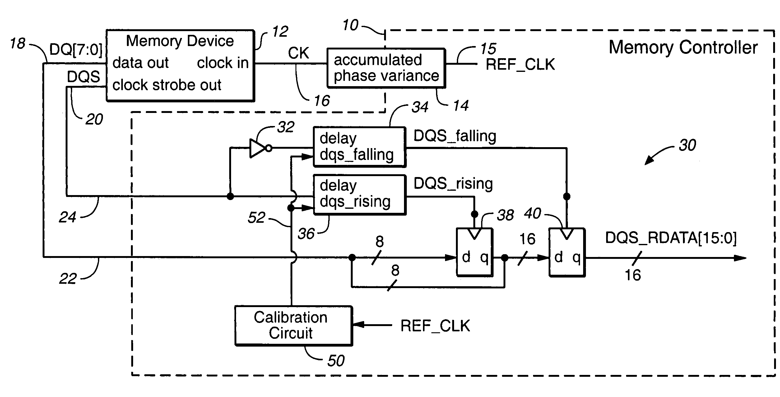
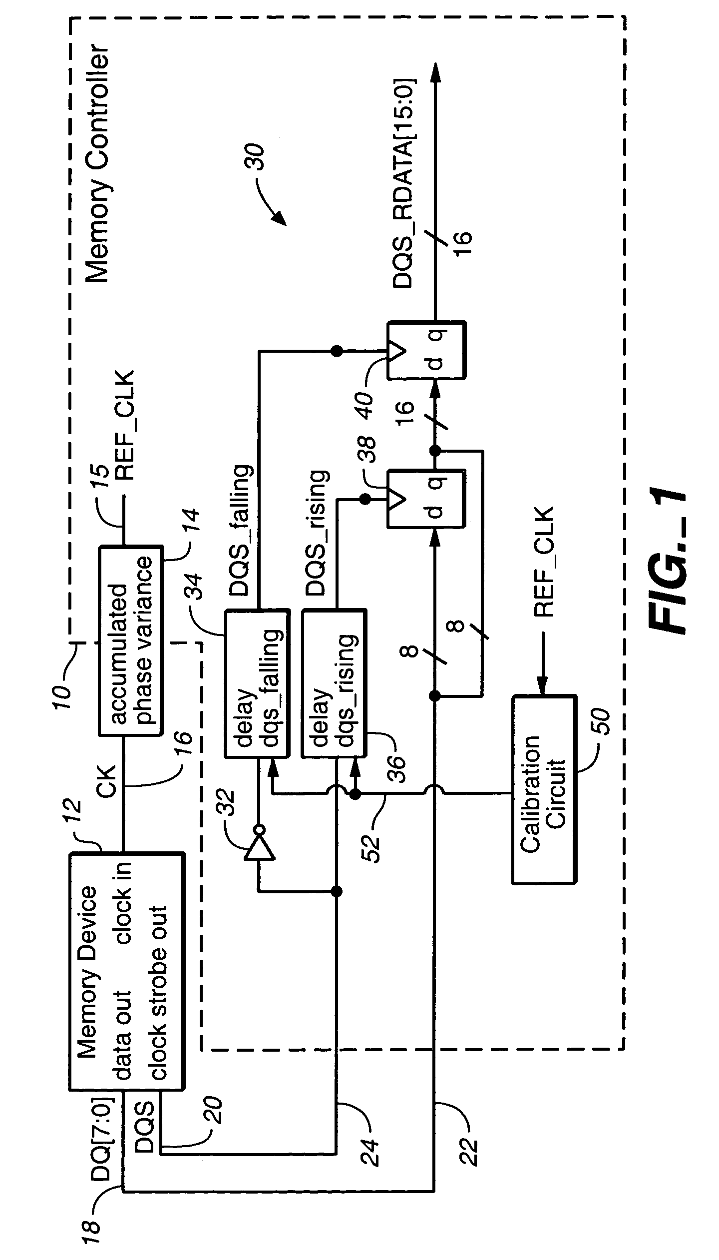
[0015]FIG. 1 is a schematic diagram illustrating an example of an application in which one embodiment of the present invention is useful. FIG. 1 illustrates a memory controller 10 coupled to a memory device 12. Memory control 10 has an internal reference clock REF_CLK, which is used for synchronizing various functions within the memory controller including the capture of data received from memory device 12 and for synchronizing read and write operations within memory device 12 through clock output 15.

[0016]In the example shown in FIG. 1, memory device 12 is a double data rate (DDR) dynamic random access memory (DRAM) having a clock input 16 labeled “CK”, an 8-bit data output 18 labeled “DQ[7:0]” and a data clock strobe output 20 labeled “DQS”. Clock input 16 is coupled to clock output 15 of memory controller 10 for receiving the memory controller's local clock signal REF_CLK. The clock signal “CK” received at clock input 16 is related to memory controller clock CLK but has an accumu...


PUM


Abstract

A delay line calibration circuit and method are provided in which a programmable master delay line drives a delay clock and has a propagation delay that is a function of a delay setting. A delay counter is clocked by the delay clock and has a delay count. A reference counter is clocked by a reference clock and has a reference count. A control circuit controls the delay and reference counters, compares a representation of the delay count to a representation of the reference count and responsively generates a modified value for the delay setting to reduce a difference between the representations of delay count and the reference count.

Description

FIELD OF THE INVENTION[0001]The present invention relates to semiconductor integrated circuits and more particularly to the calibration of a delay line to a reference clock signal.BACKGROUND OF THE INVENTION[0002]Delay lines are used within integrated circuits for a wide variety of applications, such as for adjusting or modifying the phase alignment between two signals. In one application, delay lines are used for aligning clock signals for capturing data within a data valid window. For example, certain types of memory devices generate a clock strobe signal having edges that are aligned with changes in the read data.[0003]A double data rate (DDR) dynamic random access memory (DRAM) transfers data on each rising and falling edge of the clock strobe signal. A DDR DRAM therefore transfers two data words per clock cycle. A memory controller is often used to coordinate the transfer of data to and from a memory device, such a DDR DRAM. The memory controller provides a local clock signal t...

Claims


Application Information

Patent Timeline
Patent Type & Authority Patents(United States)
IPC IPC(8): H03L7/00
CPCG11C7/1066G11C7/22G11C7/222H03L7/0995H03L7/0805H03L7/085G11C11/4076
Inventor MCCLANNAHAN, GARY P.WETZEL, DANIEL P.LIPPERT, GARY M.
Owner AVAGO TECH INT SALES PTE LTD
Learn More