
Electron beam system

a technology of electron beam and beam system, which is applied in the direction of material analysis using wave/particle radiation, instruments, nuclear engineering, etc., can solve the problems of not being able to detect defects having a size not greater than 0.2 m, and the device has been suffering from a long time-consuming inspection problem, so as to improve the yield of device manufacturing and throughput. , the effect of high reliability

Inactive Publication Date: 2007-01-02
EBARA CORP
View PDF18 Cites 27 Cited by
  • Summary
  • Abstract
  • Description
  • Claims
  • Application Information

AI Technical Summary

Benefits of technology

[0005]The present invention has been made in the light of above-pointed problems, and an object thereof is to provide an electron beam system that allows for inspection for a minute defect with high throughput and high reliability, and also to provide a device manufacturing method that can improve a yield of device manufacturing by performing the mask inspection using such a system.

Problems solved by technology

In a defect inspection apparatus of the above-described related optical system, however, any defects having a size not greater than 0.2 μm could not be detected.
Besides, although there has been one such device (an inspection apparatus of an SEM system) that allows an electron beam to scan a mask, in which secondary electrons emanated from this mask or back-scattered electrons therefrom are detected so as to inspect the mask for any potential defects therein, this device has been suffered from a problem of quite a long time being required for the inspection.

Method used


Image

  • Electron beam system
  • Electron beam system
  • Electron beam system

Examples


embodiment 2

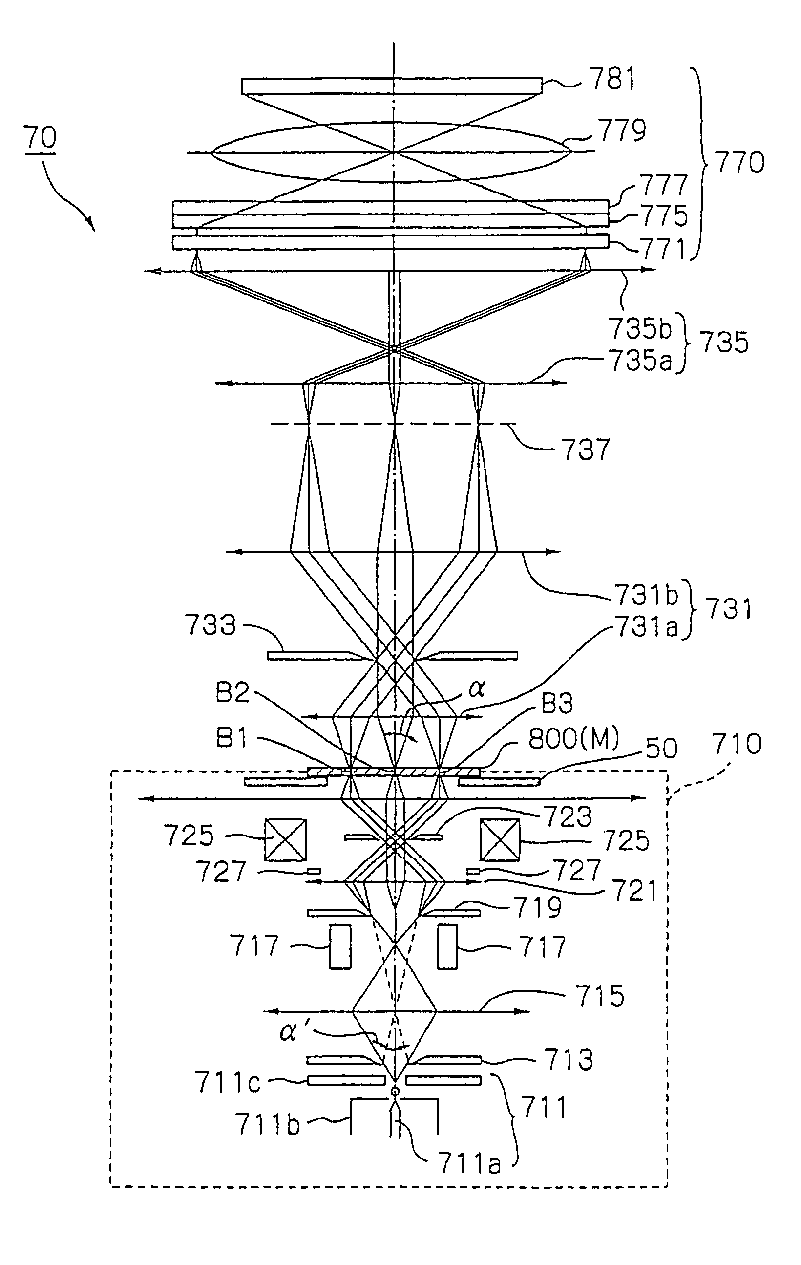
[0398]FIG. 34 shows an electron beam system according to a second embodiment of the third invention. FIG. 34 represents an electron beam system that employs a stencil mask as a sample and performs an inspection of the stencil mask. In this embodiment, an electron beam (a primary electron beam) emitted from an electron gun 212′ having an LaB6 cathode is irradiated onto a condenser lens 214′ and a shaping aperture 216′ having a rectangular opening, and the electron beam having passed through the shaping aperture 216′ is transmitted through an irradiation lens 218′ so as to be irradiated to a stencil mask 234′ prepared as the sample.

[0399]On a downstream side of the stencil mask, a first electron lens (an objective lens 232′), and in a location further downstream, a second electron lens (a magnifying lens 238′) are disposed as magnifying lenses. An electron beam transmitted through the stencil mask 234′ (a transmission electron beam) is magnified in two stages by the objective lens 232...


PUM


Abstract

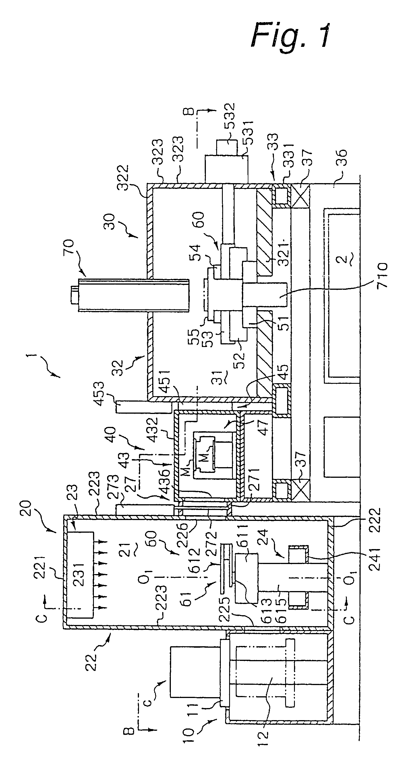
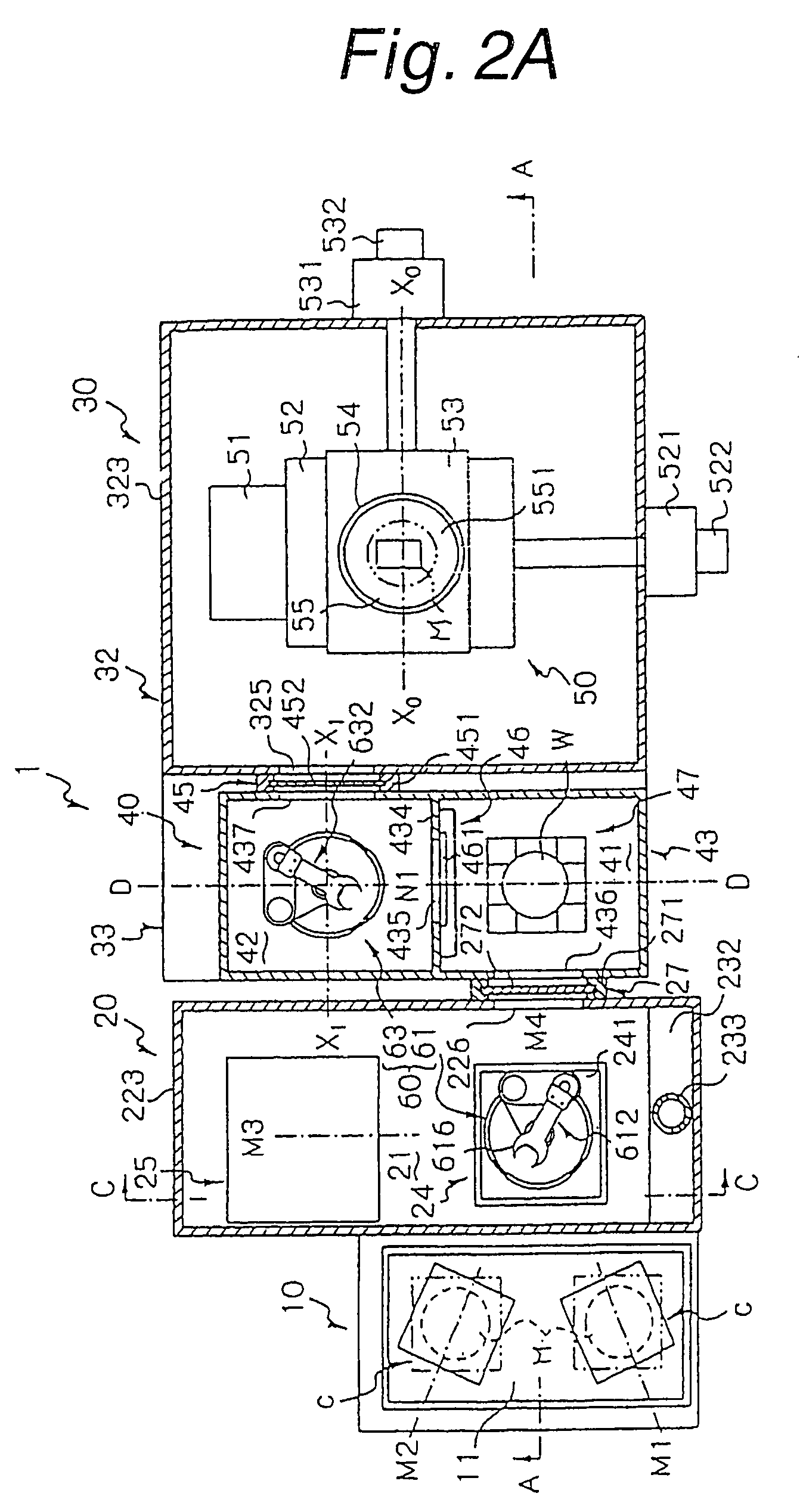
Provided is an electron beam system, in which an electron beam emitted from an electron gun is irradiated to a stencil mask, and the electron beam that has passed through the stencil mask is magnified by an electron lens and then detected by a detector having a plurality of pixels so as to form an image of the sample. Further provided is an electron beam system, in which a primary electron beam emitted from an electron gun is directed to a sample surface of a sample prepared as a subject to be inspected, and an electron image formed by a secondary electron beam emanated from the sample is magnified and detected, wherein an NA aperture is disposed in a path common to both of the primary electron beam and the secondary electron beam. An electron lens is disposed in the vicinity of a sample surface, and in this arrangement, a crossover produced by the electron gun, the electron lens and the NA aperture may be in conjugate relationships relative to each other with respect to the primary electron beam.

Description

BACKGROUND OF THE INVENTION[0001]The present invention relates to an electron beam system that can provide an evaluation, such as a defect inspection, for an electron beam transmission mask with high throughput and high reliability, and further to a manufacturing method of a device to be used in such an electron beam system.[0002]In a common practice for a defect inspection of a variety of masks including a stencil mask according to related art, a light such as a visible ray is transmitted through the mask and an image therefrom is detected by a CCD camera to thereby perform inspection (inspection by an optical system).[0003]In a defect inspection apparatus of the above-described related optical system, however, any defects having a size not greater than 0.2 μm could not be detected.[0004]Besides, although there has been one such device (an inspection apparatus of an SEM system) that allows an electron beam to scan a mask, in which secondary electrons emanated from this mask or back...

Claims


Application Information

Patent Timeline
IPC IPC(8): H01J37/26H01J37/28
CPCH01J37/28H01J2237/0492H01J2237/2817H01J2237/2446H01J2237/2806H01J2237/2441
Inventor NAKASUJI, MAMORUSATAKE, TOHRUNOJI, NOBUHARUYOSHIKAWA, SHOJIMURAKAMI, TAKESHI
Owner EBARA CORP
Learn More