Thermal imaging for semiconductor process monitoring

a technology for semiconductor process monitoring and thermal imaging, applied in the direction of heat measurement, optical radiation measurement, instruments, etc., can solve the problems of process yield limitations, inability to control process conditions adequately, and pyrometry suffers from two significant practical limitations

Inactive Publication Date: 2006-12-26
MKS INSTR INC
View PDF6 Cites 14 Cited by
  • Summary
  • Abstract
  • Description
  • Claims
  • Application Information

AI Technical Summary

Problems solved by technology

In present-day manufacturing, process yield limitations are brought about by the high sensitivity of layer properties to process conditions, and the inability to control process conditions adequately throughout the process sequence.
Pyrometry, though, suffers from two significant practical limitations.
Firstly, pyrometric sensors, traditionally employed as single point sensors, become less suitable when intra-wafer uniformity is critical.
Secondly, pyrometers require accurate knowledge of the wafer emissivity; they become unreliable or inaccurate when the emissivity is not known, when it varies during processing, or when it varies from wafer to wafer.
However, the geometric complications imposed by the reflection optics complicates the emission / reflection technique unsuitable for spatially-resolved whole wafer measurements.
The practical barriers to achieving fast and accurate temperature monitoring across large wafers is perhaps the most significant hurdle blocking broader applications of rapid thermal process technology.
In many situations however this assumption is not valid, and can lead to uncontrolled errors in temperature measurements and associated drifts in processing temperature.
Pyrometry, as it is applied in semiconductor processing, has traditionally been limited to single point measurements, with multipoint capability requiring multiple pyrometers.
Such combined emission / reflection techniques, and reflection-assisted techniques, can have excellent accuracy and precision, provided the samples are specular and opaque; however, they are poorly suited to whole wafer sensing during processing.
More particularly, although the use of reflection-assisted emissivity tracking enables extremely accurate measurement of temperature, in many applications the samples are not sufficiently specular to get a useful reflectance measurement, and geometric considerations often prohibit performing reflectance measurements on a dense point grid from a wafer in a process chamber.
Other difficulties arise, in many process situations, from the necessity to get reliable calibration reflectance reference measurements for accurate emissivity tracking.
This requires the introduction of a calibration reference of accurately known reflectance into the process chamber at very nearly the same mechanical positioning as the sample to be measured, often a difficult task and a significant practical technical barrier.

Method used


Image

  • Thermal imaging for semiconductor process monitoring
  • Thermal imaging for semiconductor process monitoring
  • Thermal imaging for semiconductor process monitoring

Examples


example one

[0037]A bare, polished, lightly doped silicon substrate, at approximately 750° C., is used for making measurements of polarized radiance, augmented by model-based analysis. At the specified temperature, the free carrier absorption is strong enough to render the wafer opaque through most of the mid infrared band, but the absorption index k is small enough that it has a negligible effect on the reflectance and emissivity; a similar situation occurs for germanium and many other semiconductors. The polarized emissivity ratio in this case is given by:

[0038]εpεs=1-ρp1-ρs=1-(n⁢⁢cos⁡(θ)-1-sin2⁡(θ) / n2n⁢⁢cos⁡(θ)+1-sin2⁡(θ) / n2)21-(⁢cos⁡(θ)-n2-sin2⁡(θ)⁢cos⁡(θ)+n2-sin2⁡(θ))2.Equation⁢⁢5

From a measurement of the PER, the index of refraction of the substrate is uniquely determined and can be computed numerically using Equation 5. With the index of refraction of the substrate calculated from Equation 5, the emissivities in the two orthogonal polarizations can be computed, and the radiance can be re...

example two

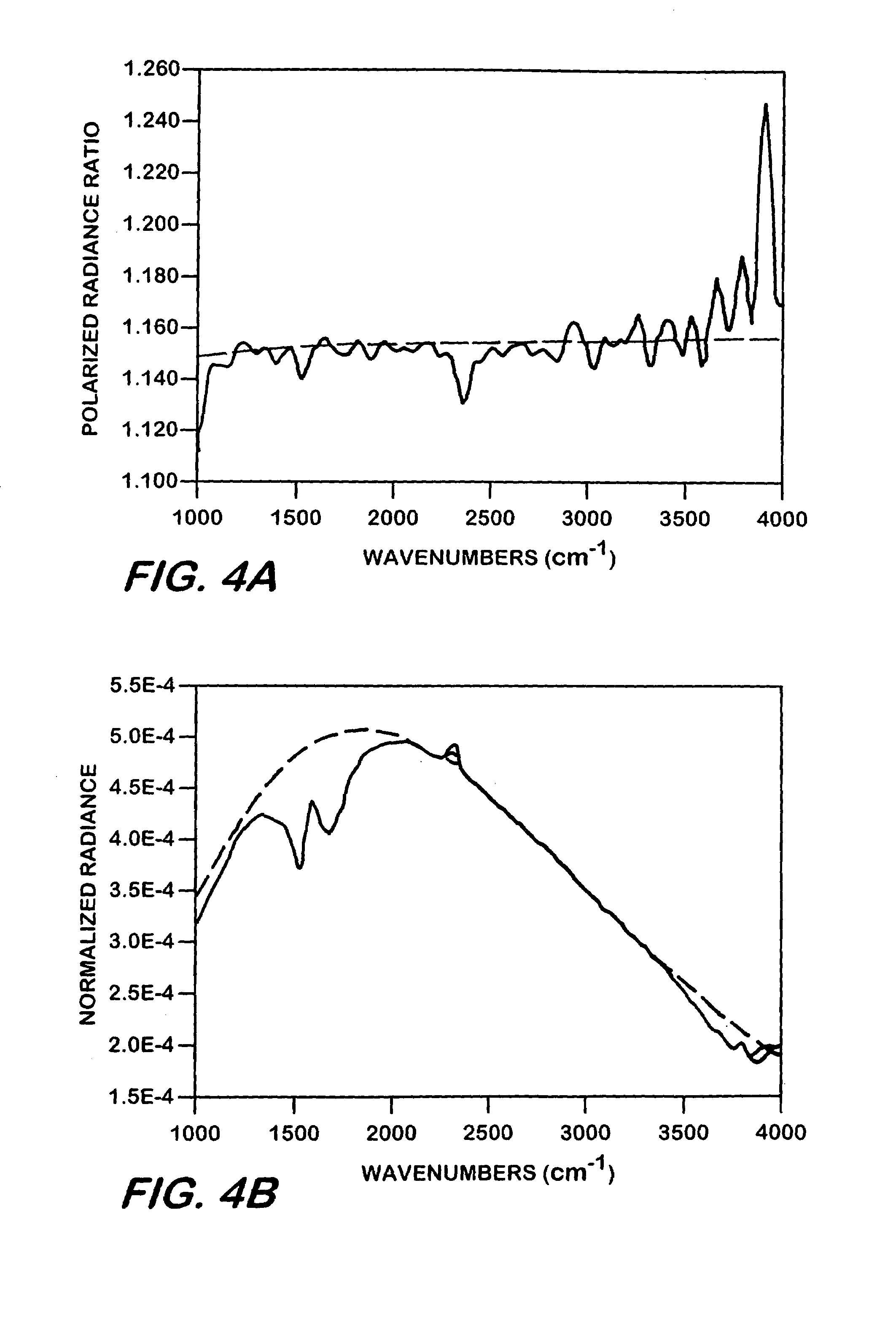
[0042]As a second example, it is demonstrated that the instant method can be generalized to more complex situations, including samples with overlayers. Taking, in this instance, a hot silicon wafer carrying thin silicon dioxide film, the polarized radiance ratio, measured with an FT-IR at a take-off angle of 30°, is shown in FIG. 5(a). This spectrum was fit to a model in which the silicon oxide thickness was varied, and the optical constants of the silicon and silicon oxide were approximated by their room temperature values. FIG. 5(a) also shows the overlayed fit. The thickness was determined from the fit to be given by 0.48 micron. Using the now known thickness and the optical constants of the silicon substrate and the silicon oxide overlayer, the emissivity was calculated using a transfer matrix formalism similar to that described by Springthorpeet al. (A. J. Springthorpe, T. P. Humphreys, A Majeed, and W. T. Moore, Applied Phys. Lett. 55, (2), pp 2138–2140, 1989). The radiance sp...

example three

[0044]A third example of the method employs a sample having a non-specular surface, i.e., a sample that is relatively smooth on a macroscopic scale but rough enough to be a diffuse scatterer at infrared wavelengths, a situation that is often encountered when measuring the backsides of the single-side polished silicon wafers that are commonly employed in semiconductor manufacturing. In such a case, the sample is assumed to be specular, from the point of view of emission, with the effect of the sample roughness being largely to provide a distribution of takeoff angles from a given measurement spot. If this distribution is sufficiently narrow, as it commonly is for modern silicon wafers, then the emissivity is sufficiently well described by the average takeoff angle to provide an accurate emissivity and temperature measurement.

[0045]FIG. 6(a) shows a measurement of the polarized radiance ratio from a hot, smooth, but non-specular, silicon wafer backside at a 30° take-off angle, overlay...


PUM

PropertyMeasurementUnit
temperatureaaaaaaaaaa
takeoff angleaaaaaaaaaa
temperatureaaaaaaaaaa

Abstract

The method measures the temperature, emissivity, and other properties of relatively smooth surfaces radiating thermal energy, and is especially adapted for monitoring semiconductor fabrication processes. Temperature is determined by relating measured radiance to the predictions of the Planck radiation law, using knowledge of the emissivity determined from an analysis of the polarization of the thermally emitted radiance. Additional information regarding the properties of thin films, such as thickness and composition, can be computed from the emissivity or the ratio of the emissivities measured at two independent polarizations. Because the data are obtained from the intrinsic thermal radiance, rather than from an extrinsic light source, the measurement can be performed when it is inconvenient or impossible to provide a light source for reflectance measurements.

Description

CROSS-REFERENCE TO RELATED PROVISIONAL APPLICATION[0001]This application claims the benefit of provisional Application No. 60 / 067,202, bearing the foregoing title and filed on Dec. 1, 1997 in the names of the inventors designated herein.STATEMENT REGARDING GOVERNMENT INTEREST[0002]The United States Government has rights in this invention under Department of Defense Contract No. F 33615-97-C-5134.BACKGROUND OF THE INVENTION[0003]The production of future generations of submicron VLSI silicon microelectronics and compound semiconductor devices will depend critically on continued advances in process sensing and control. In present-day manufacturing, process yield limitations are brought about by the high sensitivity of layer properties to process conditions, and the inability to control process conditions adequately throughout the process sequence. Present technology relies primarily upon the inference of important process parameters from indirect sensor signals, and upon open-loop cont...

Claims


Application Information

Patent Timeline
Patent Type & Authority Patents(United States)
IPC IPC(8): G01K11/00G06F15/00G01J5/00G01J5/58G01J5/60
CPCG01J5/0003G01J5/58G01J5/60
Inventor ROSENTHAL, PETER A.XU, JIAZHANCHARPENAY, SYLVIECOSGROVE, JOSEPH E.
Owner MKS INSTR INC
Why Eureka
Try Eureka