
Design tool for systems-on-a-chip

a design tool and system-on-a-chip technology, applied in the direction of cad circuit design, program control, instruments, etc., can solve the problems of increasing the difficulty of a single company to provide its customers with all of the semiconductor intellectual property, the complexity is inversely proportional, and so as to reduce the time-to-market of users and develop quickly

Inactive Publication Date: 2006-10-17
NETVINCI
View PDF16 Cites 95 Cited by
  • Summary
  • Abstract
  • Description
  • Claims
  • Application Information

AI Technical Summary

Benefits of technology

[0016]An advantage of the present invention is that a system is provided that enables electronics applications to be developed quickly and to be portable between silicon foundries.

Problems solved by technology

As systems-on-chip (SoC) become more complex, it will be increasingly difficult for a single company to provide its customers with all of the semiconductor intellectual property (SIP) cores and library macrocells they require.
SoC's are reaching higher levels of integration, but their complexity is inversely proportional to the allowable time-to-market.
But just purchasing the semiconductor intellectual property is not enough.
Integrating semiconductor intellectual property in a system-on-chip is complicated, especially when components from multiple sources are involved.
At the board level, a key issue is minimizing the number of bus signals because pin and signal count translate directly into package and PCB costs.
A large number of device pins increases the package footprint and reduces component density on the board.
The limited capabilities of today's logic synthesis tools directly impact embodiment time and performance and must be taken into account.
Getting the lowest possible routing overhead is of little value if the system design time balloons way out of proportion and the market window is missed.
Synthesis tools find it difficult to deal with shared tri-state signals with several drivers and receivers connected to the same trace.
Static timing analysis is preferably awkward, and often the only way to verify timing is to use a circuit level simulator, e.g., SPICE.
All of this takes time and effort without adding real value in terms of device functionality or features.
Bus loading also limits theoretical performance and the verification problems associated with bus loading can lead to a conservative embodiment whose performance falls short of the inherent technology capabilities.

Method used


Image

  • Design tool for systems-on-a-chip
  • Design tool for systems-on-a-chip
  • Design tool for systems-on-a-chip

Examples


Embodiment Construction

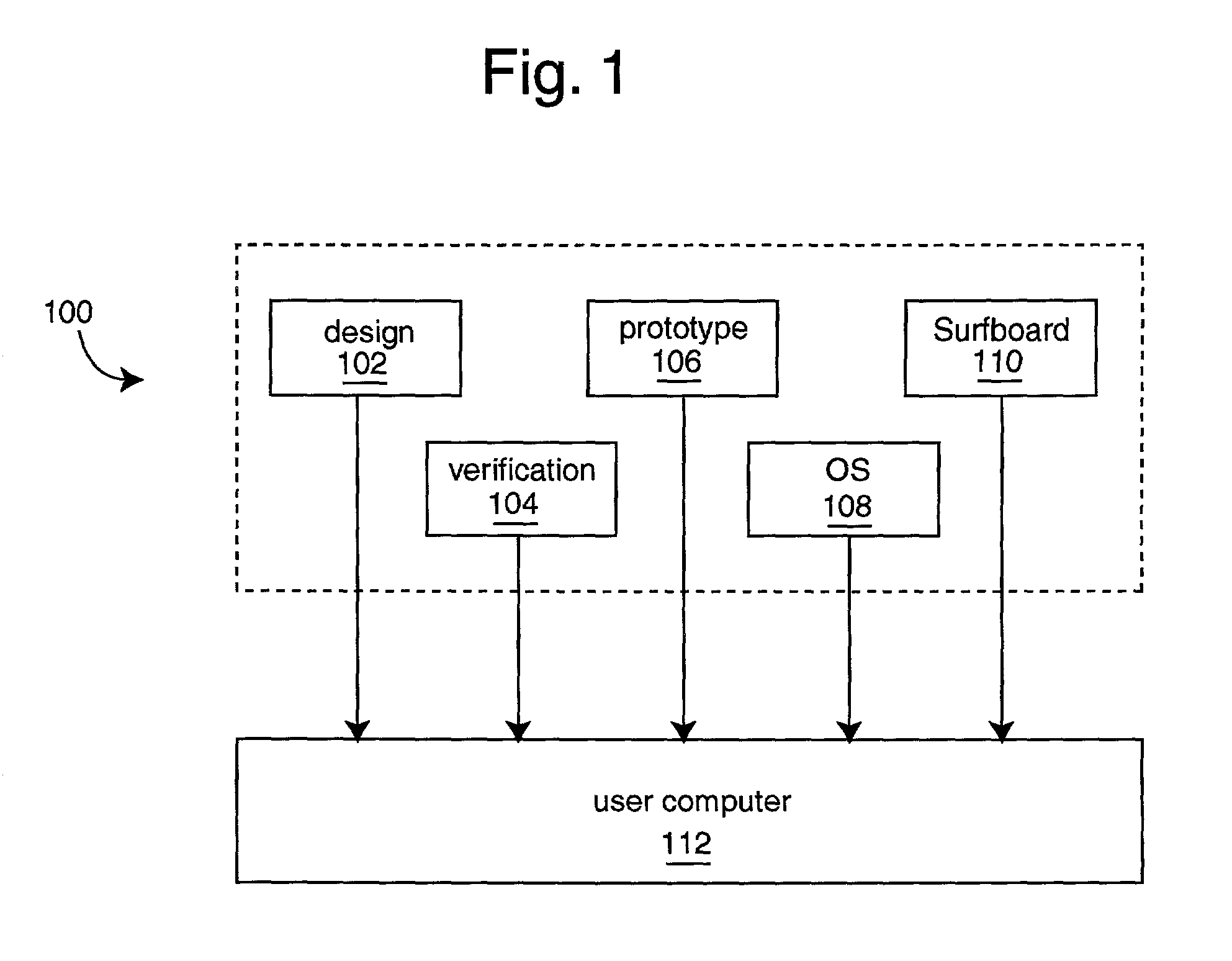
[0024]FIG. 1 illustrates a system-on-chip (SoC) design platform embodiment of the present invention for system-on-chip integration, and is referred to by the general reference numeral 100. The SoC design platform 100 is delivered to a user that include design 102, verification 104, prototype 106, operating system (OS) 108, and Palmchip Corporation (San Jose, Calif.) Surfboard 110.

[0025]The design, verification, prototype, and operating system deliverables 100, 102, 104, 106, and 108, are embodied as electronic data and may be delivered as computer data files. Such computer-data files are carried on removable disk or downloaded over the Internet for a subscription or usage fee. For example, an Internet-based SIP sales and delivery system is the so-called Virtual Component Exchange (VCX), see www.vcx.org. The SoC design platform 100 enables users to co-develop target hardware and software that integrates standard SIP-blocks with their own value-added SIP-blocks.

[0026]The basic SoC bui...


PUM


Abstract

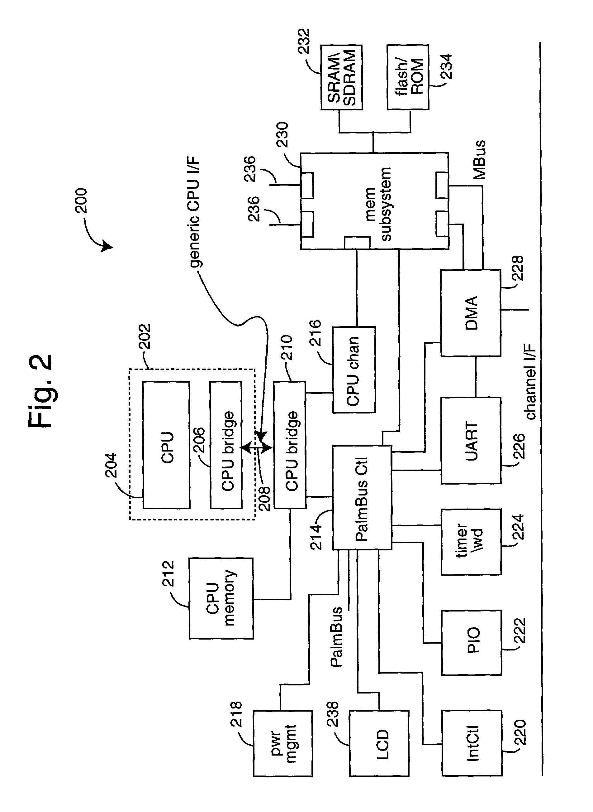
A pre-designed system-on-chip architecture and method includes several standard library devices, HDL source code, simulation environment and regression, synthesis scripts, software header files, software libraries, ASIC verification test suites, and makefiles. The standard library devices comprise an integrated CPU, a shared memory controller, a peripheral controller, system peripherals, a DMA controller, embedded memory, and general system control. CPU bridges are used to accommodate a variety of processor types and to insulate users from the complexities of interfacing to different kinds of processors. Such CPU bridges further allow the latest processors to be rapidly integrated into existing integration platforms and designs.

Description

COPENDING APPLICATION[0001]This patent application is a continuation-in-part of U.S. patent application Ser. No. 09 / 565,282, filed May 2, 2000, and titled CHIP-CORE FRAMEWORK FOR SYSTEMS-ON-A-CHIP, by S. Jauher A. ZAIDI, et al.BACKGROUND OF THE INVENTION[0002]1. Field of the Invention[0003]The present invention relates generally to semiconductor integrated circuit design and devices, and more specifically to pre-designed system-on-chip architectures with HDL source code, simulation environment and regression, synthesis scripts, software header files, software libraries, ASIC verification test suite, and makefiles.[0004]2. Description of the Prior Art[0005]As systems-on-chip (SoC) become more complex, it will be increasingly difficult for a single company to provide its customers with all of the semiconductor intellectual property (SIP) cores and library macrocells they require. Companies have to evaluate whether human resources, capital and time are expendable on extraneous developm...

Claims


Application Information

Patent Timeline
IPC IPC(8): G06F17/50G06F13/38
CPCG06F13/38G06F13/28G06F2217/66G06F2115/08
Inventor ZAIDI, S. JAUHER A.OU, MICHAELADAMS, LYLE E.CHAPPELL, STEPHENGANDIKOTA, SAVITHAUDELL, JONGUTCHER, BRIANMUNSIL, JEF
Owner NETVINCI
Learn More