
Shared bit line memory device and method

a bit line memory and shared technology, applied in the field of digital memories, can solve the problems of limiting the degree of integration and miniaturization possible, limiting the device size and density, and complex nature of the interconnection of the array of bit-cells

Inactive Publication Date: 2006-08-15
SHEPPARD DOUGLAS P
View PDF7 Cites 86 Cited by
  • Summary
  • Abstract
  • Description
  • Claims
  • Application Information

AI Technical Summary

Benefits of technology

[0012]In a refinement of the foregoing invention, the number of word-lines aligned with each of the plural rows is an integer number that is greater than one. In particular, that number may be a power of two. In a specific embodiment of the invention, the memory is arranged such that no two bit-cells within each of the discrete fractions of the plural bit-cells along any given row are positioned adjacent to one another. In another embodiment of t

Problems solved by technology

Due to cost, yield, and performance issue that surround the design and manufacture of memory devices, designers are continually challenged to implement logic and schematic designs in an efficient design realizable in a physical memory device.
In fact, the conversion of a schematic memory design to a physical device design is the essential challenge in memory design.
When designers generate memory integrated circuit layouts, the space available on the Contact and Metal-1 layers are at a premium and can be a limiting factor in device size and density.
Several design rules known to those skilled in the art limit the degree of integration and miniaturization possible.
Another aspect in the design of high-density memory device is the complex nature of the interconnection of the array of bit-cells to the associated addressing, decoding and read / write access circuitry.
Thus, power consumption in the active state of accessing a memory cell is proportional the number of traces and circuit elements that are being driven over the voltage change of the read or write operation in progress.
Notwithstanding the improvements in the prior art, there still exist practical limits on memory array circuit density in the prior art.
The advantages of reduced die size, including lower parts cost and higher manufacturing yields, cannot be realized because of the high number of traces and circuit interconnections required in prior art memory array integrated circuit designs.
In the case of multiple port memory devices, this problem is exacerbated.

Method used


Image

  • Shared bit line memory device and method
  • Shared bit line memory device and method
  • Shared bit line memory device and method

Examples


Embodiment Construction

[0045]Illustrative embodiments and exemplary applications will now be described with reference to the accompanying drawings to disclose the advantageous teachings of the present invention.

[0046]While the present invention is described herein with reference to illustrative embodiments for particular applications, it should be understood that the invention is not limited thereto. Those having ordinary skill in the art and access to the teachings provided herein will recognize additional modifications, applications, and embodiments within the scope thereof and additional fields in which the present invention would be of significant utility.

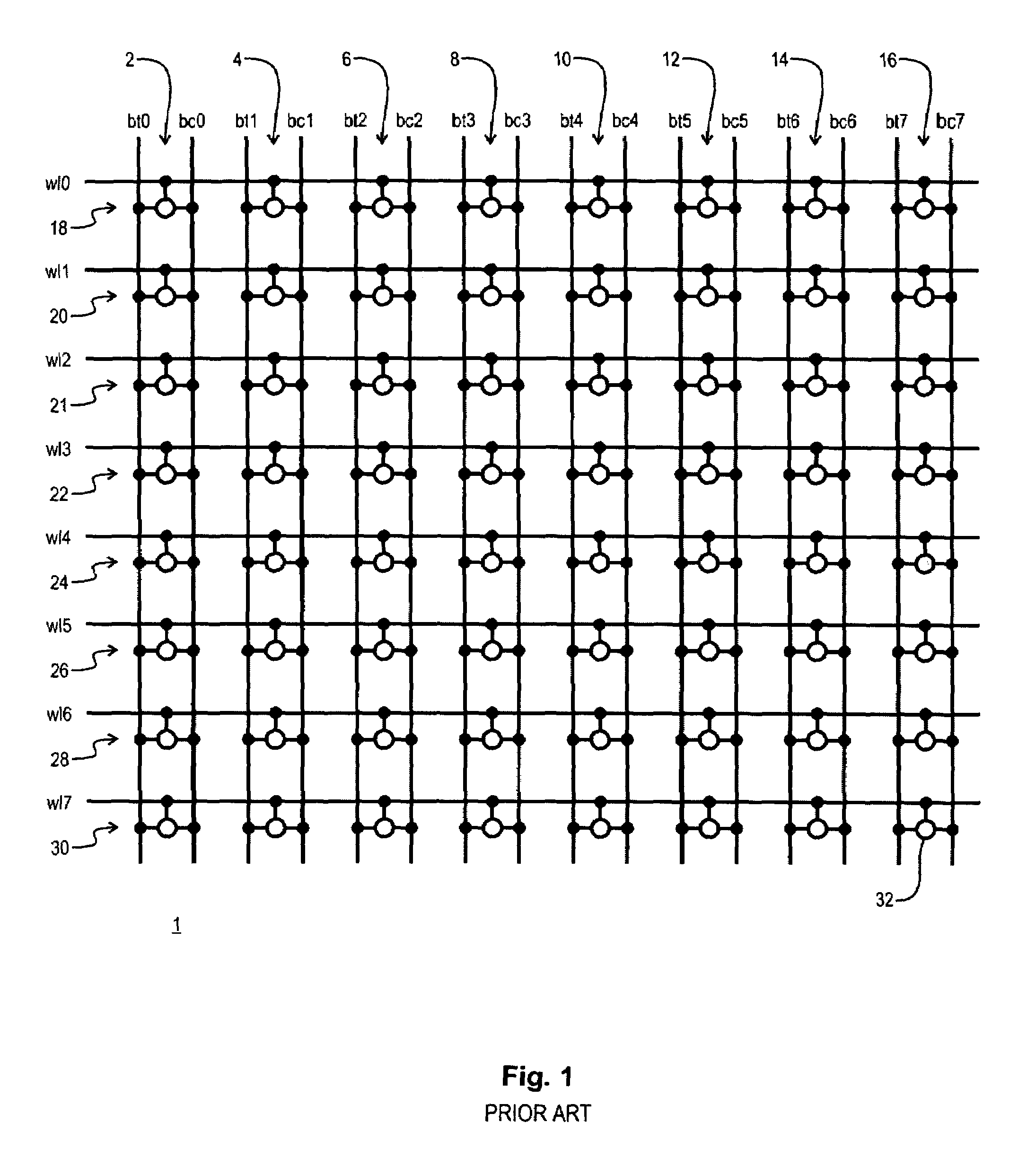
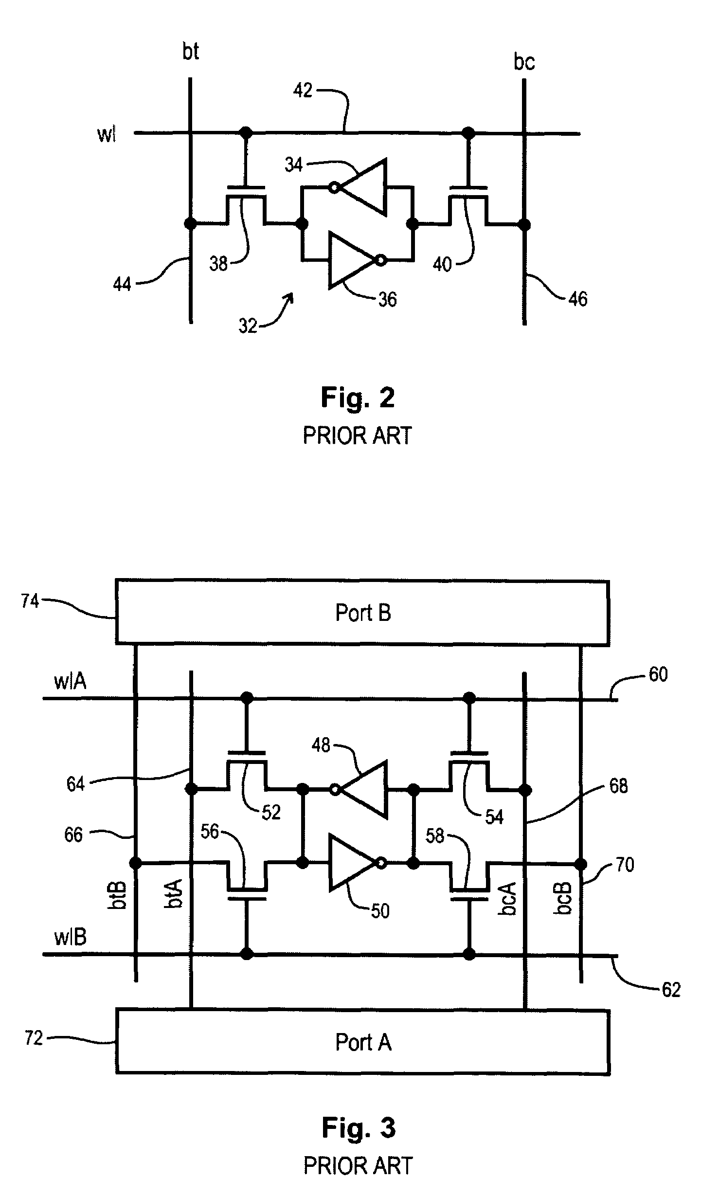
[0047]A detailed description of the present invention begins with a description of prior art memory array designs that existed before the advent of Multiple Word Line technology. Next, is a brief description of the advancements brought by the Multiple Word Line technology, which are taught in the related patent application filed by the inventor of th...


PUM


Abstract

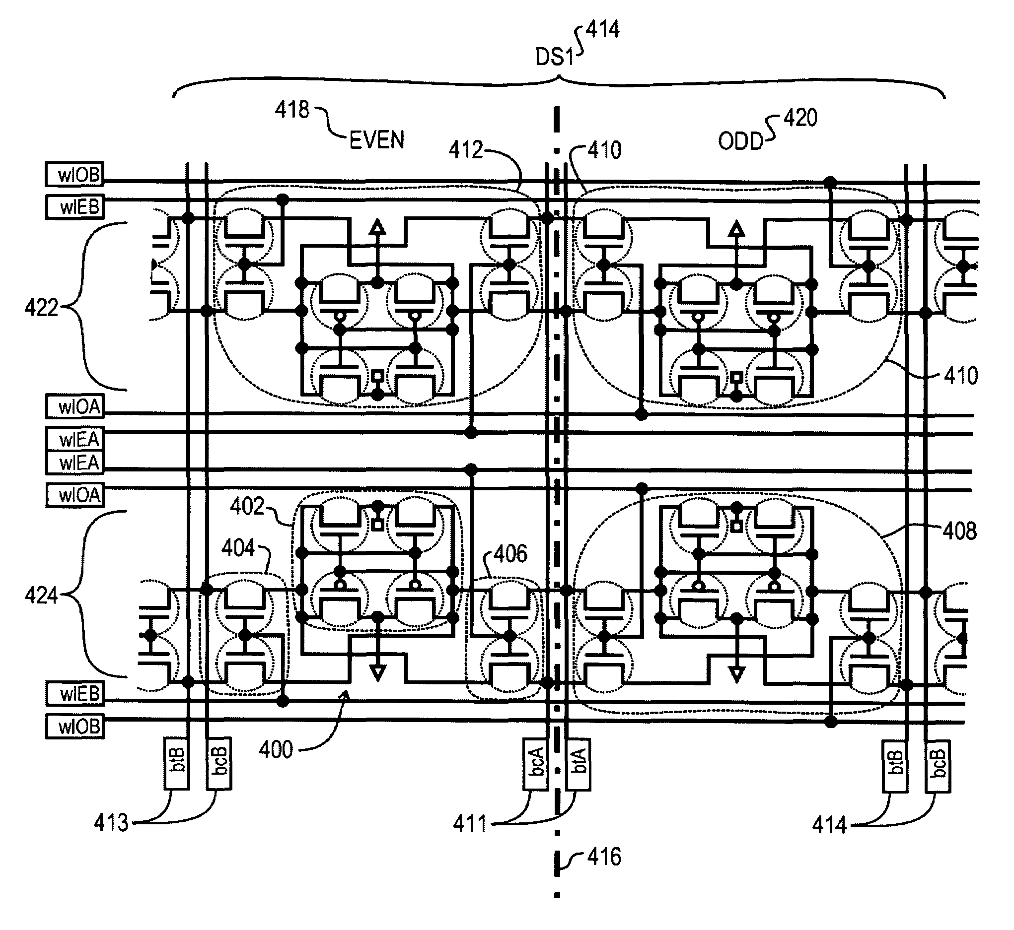
A memory array employing shared bit-lines. A memory is formed from an array of plural bit-cells organized as plural columns and plural rows. Plural word-lines are aligned with each for the rows, and each is electrically coupled to a discrete fraction of the bit-cells its corresponding row. The memory also includes plural bit-lines that are aligned with the plural columns. Every bit-line is electrically coupled to all of the bit-cells that lie along at least one column. In addition, at least a first one of the bit-lines is further electrically coupled to all of the bit-cells in an additional column. That bit-line is coupled such that every one of the plural bit-cells, that lie along any given row that are coupled to it, is coupled to a unique word-line from the other bit-cells coupled thereto. The shared bit-line invention is applicable to single and multiple port memory arrays. It is applicable to all memory array technologies including, but not limited to, SRAMs and DRAMs.

Description

RELATED APPLICATION DATA[0001]Continuation-in-part of Ser. No. 10 / 395,312, filed Mar. 24, 2003, abandoned.BACKGROUND OF THE INVENTION[0002]1. Field of the Invention[0003]The present invention relates to digital memories. More specifically, the present invention relates digital memory arrays organized in rows and columns and used in various digital devices.[0004]2. Description of the Related Art[0005]Modern computing devices utilize a variety of kinds of memory devices to store and access information. Several memory device technologies are familiar to those skilled in the art and include the general classes of random access memories (“RAM”) and read only memories (ROM”). These classes further comprise static RAM (“SRAM”), dynamic RAM (“DRAM”), programmable ROM (“PROM”), erasable PROM (“EPROM”), electrically erasable PROM (“EEPROM”), as well as FLASH memory, smaller register files, and other memory types known to those skilled in the art. Most memory devices employ an internal archite...

Claims


Application Information

Patent Timeline
IPC IPC(8): G11C11/00
CPCG11C7/02G11C7/18G11C8/16H01L27/11H01L27/10882G11C11/412H01L27/0207H10B12/48H10B10/00
Inventor SHEPPARD, DOUGLAS P.
Owner SHEPPARD DOUGLAS P
Learn More