
Semiconductor light emitting element and method of making same

a light-emitting element and semiconductor technology, applied in the direction of semiconductor devices, basic electric elements, electrical appliances, etc., can solve the problems of unsatisfactory voids, complicated semiconductor crystal growth process, difficult to obtain good semiconductor crystals, etc., to achieve simplified and shorten the crystal growth process

Inactive Publication Date: 2006-08-08
TOYODA GOSEI CO LTD
View PDF13 Cites 17 Cited by
  • Summary
  • Abstract
  • Description
  • Claims
  • Application Information

AI Technical Summary

Benefits of technology

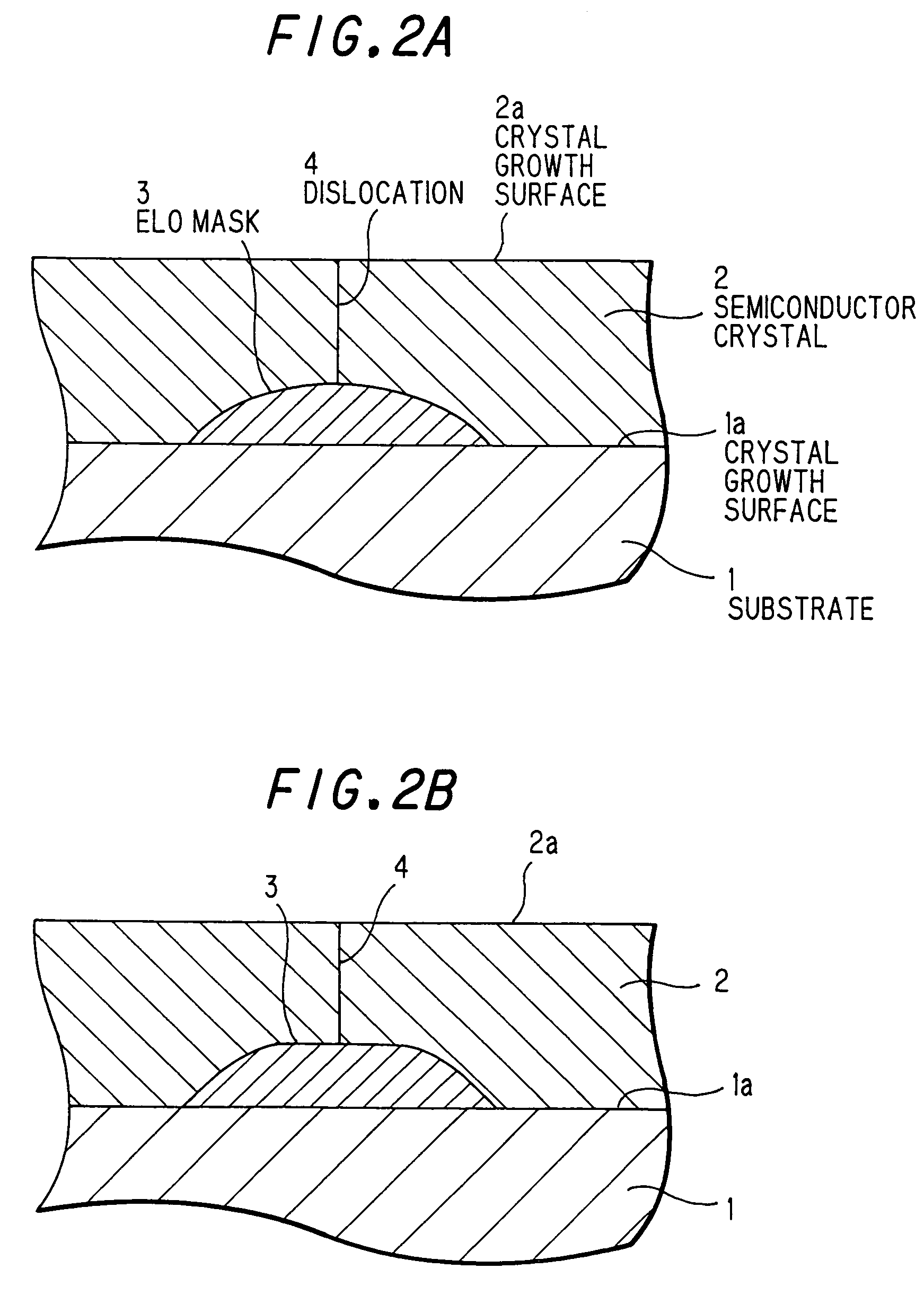
The invention provides a method for making a semiconductor light emitting element that simplifies the crystal growth process and reduces voids in the crystal. Additionally, the invention improves the external and internal quantum efficiency of the semiconductor light emitting element. This is achieved by using the lateral growth function of semiconductor crystal and an ELO mask with an inclined plane that is inclined to the crystal growth surface. The method involves forming an ELO mask on a crystal growth substrate, providing an inclined plane on at least part of the sidewall of the ELO mask, and growing semiconductor crystal on the crystal growth substrate.

Problems solved by technology

There may occur a problem in subsequent alignment step.
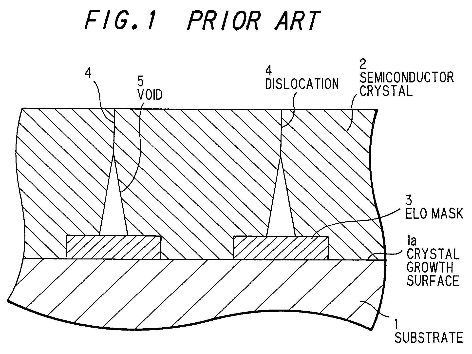
Further, in aspect of external quantum efficiency, it is undesirable to have such a void since part of light emitted from a light emitting element formed on the semiconductor crystal 2 may be diffused by such a void.
These requirements may further complicate the semiconductor crystal growth process for light emitting element that is complicated recently.
Namely, in case of using these methods, it is difficult to obtain a good semiconductor crystal while simplifying the crystal growth process.

Method used


Image

  • Semiconductor light emitting element and method of making same
  • Semiconductor light emitting element and method of making same
  • Semiconductor light emitting element and method of making same

Examples


examples

[0090]In examples below, (1) ELO mask process and (2) crystal growth process that can be directly applied to a method of making a semiconductor light emitting element will be described.

(1) ELO Mask Process

[0091]FIGS. 5A to 5F are schematic cross sectional views showing a process of making an ELO mask 3 in the preferred embodiment of the invention.

(A) Plasma CVD Step [FIG. 5A]

[0092]First, a crystal growth substrate 1 of sapphire is provided. Asapphirea-faceisusedasa crystal growth surface 1a. Then, ELO mask prototype layer 3″ of SiO2 is grown about 1.0 μm on the crystal growth surface 1a (sapphire a-face) by using a microwave plasma CVD device.

[0093]The operation conditions of plasma CVD device as well as the flow rate of source gases are as follows:

[0094]Pressure: 70 Pa

[0095]Substrate Temperature: 300° C.

[0096]Microwave Output: 50 W

[0097]SiH4 (8%): 25 sccm

[0098]N2O: 150 sccm

[0099]N2: 500 sccm

(B) Photoresist Coating Step [FIG. 5B]

[0100]Then, a photoresist layer 6 is coated about 1.6 ...


PUM


Abstract

A semiconductor light emitting element that is made by using the lateral growth function of semiconductor crystal while providing an ELO mask on a crystal growth surface of a crystal growth substrate. At least part of a sidewall of the ELO mask is provided with an inclined plane that is inclined to the crystal growth surface such that the semiconductor crystal to be formed on the ELO mask substantially has no void.

Description

[0001]The present application is based on Japanese patent application No. 2003-090884, the entire contents of which are incorporated herein by reference.BACKGROUND OF THE INVENTION[0002]1. Field of the Invention[0003]The invention relates to a method of making a semiconductor crystal by using an ELO (epitaxial lateral overgrowth) mask of amorphous material formed on a crystal growth surface to offer lateral growth of crystal. Also, the invention relates to a semiconductor light emitting element made by using the method.[0004]2. Description of the Related Art[0005]Several methods of reducing a dislocation or void in the crystal to make a good semiconductor crystal by using an ELO mask are known (e.g., prior arts 1 to 4 below).[0006]Japanese patent application laid-open No. 2000-21789 (prior art 1) discloses that the number of voids or cracks can be relatively reduced by using an ELO mask formed on an underlying layer of AlGaN.[0007]Japanese patent application laid-open No. 2000-35766...

Claims


Application Information

Patent Timeline
Patent Type & Authority Patents(United States)
IPC IPC(8): H01L27/15H01L21/20H01L21/205H01L33/32
CPCH01L33/007H01L21/02647H01L21/02378H01L21/02381H01L21/02389H01L21/0262H01L21/02458H01L21/0254H01L21/02576H01L21/02579H01L21/0242
Inventor SENDA, MASANOBUITO, JUNNISHIJIMA, KAZUKIHAYASHI, TOSHIMASA
Owner TOYODA GOSEI CO LTD
Learn More