
Formation of finFET using a sidewall epitaxial layer

a technology of sidewall epitaxial layer and fin fet, which is applied in the direction of electrical equipment, semiconductor devices, medical science, etc., can solve the problems of degrading the ability of the gate of the same to control whether, becoming increasingly difficult, and suffering from several problems in the conventional mos

Inactive Publication Date: 2006-07-18
ADVANCED MICRO DEVICES INC
View PDF8 Cites 118 Cited by
  • Summary
  • Abstract
  • Description
  • Claims
  • Application Information

AI Technical Summary

Benefits of technology

The patent text describes methods for making strained silicon finFETs using a sidewall epitaxial layer. These methods involve depositing layers of silicon germanium (SiGe) and a cap layer above an oxide layer on a substrate, patterning the layers to form a gate structure, and selectively etching to remove the gate structure and leave the strained silicon sidewalls to define strained silicon structures. The resulting strained silicon structures have improved performance and can be used in integrated circuits. The technical effects of this patent text are improved performance and reliability of strained silicon structures in integrated circuits.

Problems solved by technology

This is generally referred to as device “scaling.” As MOSFETs are scaled to channel lengths below 100 nm, conventional MOSFETs suffer from several problems.
In particular, interactions between the source and drain of the MOSFET degrade the ability of the gate of the same to control whether the device is on or off.
As device size is scaled, however, this becomes increasingly difficult because the distance between the source and drain is reduced.

Method used


Image

  • Formation of finFET using a sidewall epitaxial layer
  • Formation of finFET using a sidewall epitaxial layer
  • Formation of finFET using a sidewall epitaxial layer

Examples


Embodiment Construction

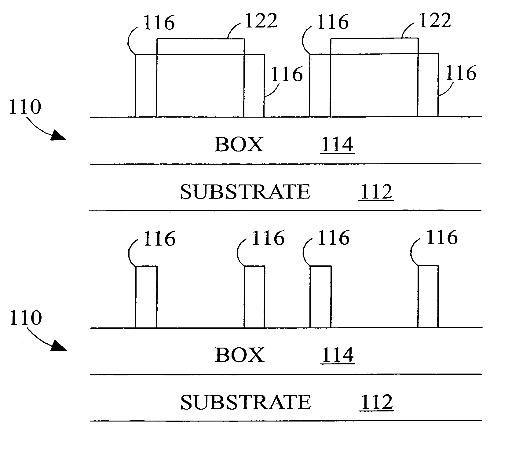
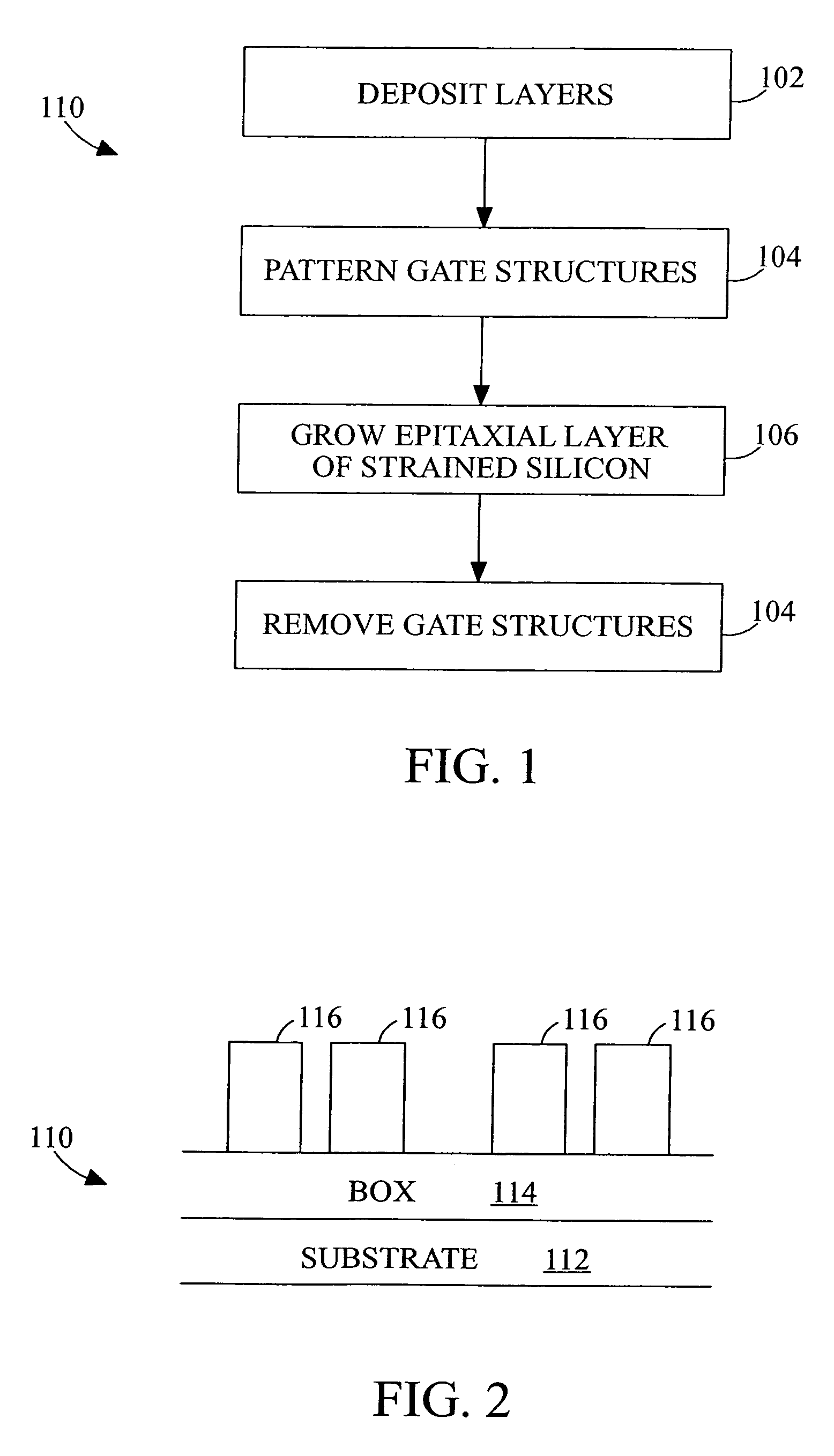
[0022]With reference to FIG. 1, an advantageous process 100 forms strained silicon finFET structures using a sidewall epitaxial layer. The strain in these finFET structures can be used to enhance electron mobility. While process 100 is described by way of example, additional, fewer, or different operations may be performed. Process 100 is not limited to the operations, materials, or techniques described herein.

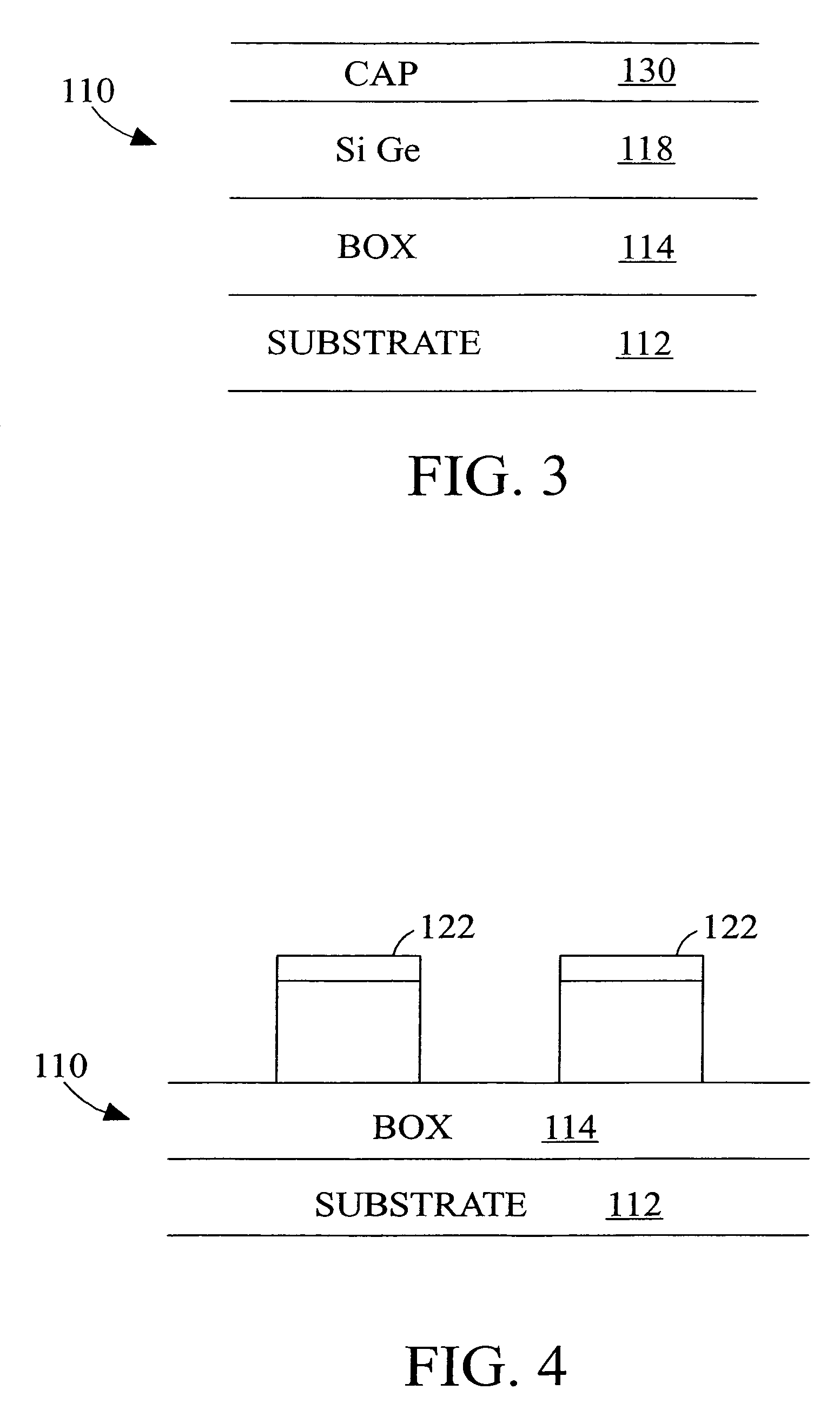
[0023]In an operation 102, various layers are formed over a substrate. For example, a buried oxide layer is formed above a substrate and a silicon germanium layer (SiGe) layer is formed above the buried oxide layer. The silicon germanium (SiGe) layer can be deposited above the buried oxide layer using any of a variety of deposition techniques. A cap layer can be deposited above the silicon germanium layer.

[0024]In an operation 104, gate structures are patterned from the silicon germanium layer and cap layer provided in operation 102. Structures can be patterned from the silico...


PUM


Abstract

A method of forming a finFET transistor using a sidewall epitaxial layer includes forming a silicon germanium (SiGe) layer above an oxide layer above a substrate, forming a cap layer above the SiGe layer, removing portions of the SiGe layer and the cap layer to form a feature, forming sidewalls along lateral walls of the feature, and removing the feature.

Description

FIELD OF THE INVENTION[0001]The present invention is related to integrated circuit (IC) devices. More particularly, the present invention relates to a method of forming a strained silicon FIN FET using a sidewall epitaxial layer.BACKGROUND OF THE INVENTION[0002]Metal-Oxide-Semiconductor Field Effect Transistor (MOSFET) technology is well known and widely used in the electronics industry. Performance enhancement between generations of devices is generally achieved by reducing the size of the device, resulting in an enhancement in device speed. This is generally referred to as device “scaling.” As MOSFETs are scaled to channel lengths below 100 nm, conventional MOSFETs suffer from several problems. In particular, interactions between the source and drain of the MOSFET degrade the ability of the gate of the same to control whether the device is on or off. This phenomenon is called the “short-channel effect”.[0003]Silicon-on-insulator (SOI) MOSFETs are formed with an insulator (usually,...

Claims


Application Information

Patent Timeline
Patent Type & Authority Patents(United States)
IPC IPC(8): H01L21/336A61F5/37H01L29/10H01L29/786
CPCA61F5/3776H01L29/1054H01L29/785H01L29/78687H01L29/66795Y10S438/933
Inventor MASZARA, WITOLD P.GOO, JUNG-SUKPAN, JAMES N.XIANG, QI
Owner ADVANCED MICRO DEVICES INC
Learn More