Method for fabricating non-volatile memory

a non-volatile memory and fabrication method technology, applied in the direction of semiconductor devices, basic electric elements, electrical appliances, etc., can solve the problem of inability to increase the integration level, achieve the effect of simplifying the process, reducing cost, and increasing the integration level and efficiency of devices

Active Publication Date: 2006-07-04
POWERCHIP SEMICON MFG CORP
View PDF6 Cites 36 Cited by
  • Summary
  • Abstract
  • Description
  • Claims
  • Application Information

AI Technical Summary

Benefits of technology

[0011]Accordingly, the present invention is directed to a fabrication method of a non-volatile memory to increase the level of integration and efficiency of the devices with simplified process and reduced cost.
[0031]In accordance to the fabrication method for the non-volatile memory of the present invention, there is no demand for the lithography and etching processes for forming the gate structures between the stacked gate structures. Therefore, the fabrication process is simplified and the cost is reduced. On the other hand, the first memory cell constituted by the first gate and the second memory cell constituted by the second gate share the first dielectric layer and the charge trapping layer. Not only the fabrication process is simplified, the quality of the bottom oxide layer for the second memory cell, which is always undesirable when formed with the conventional method, is also improved.

Problems solved by technology

Therefore, the level of integration can not be increased.

Method used


Image

  • Method for fabricating non-volatile memory
  • Method for fabricating non-volatile memory
  • Method for fabricating non-volatile memory

Examples


Embodiment Construction

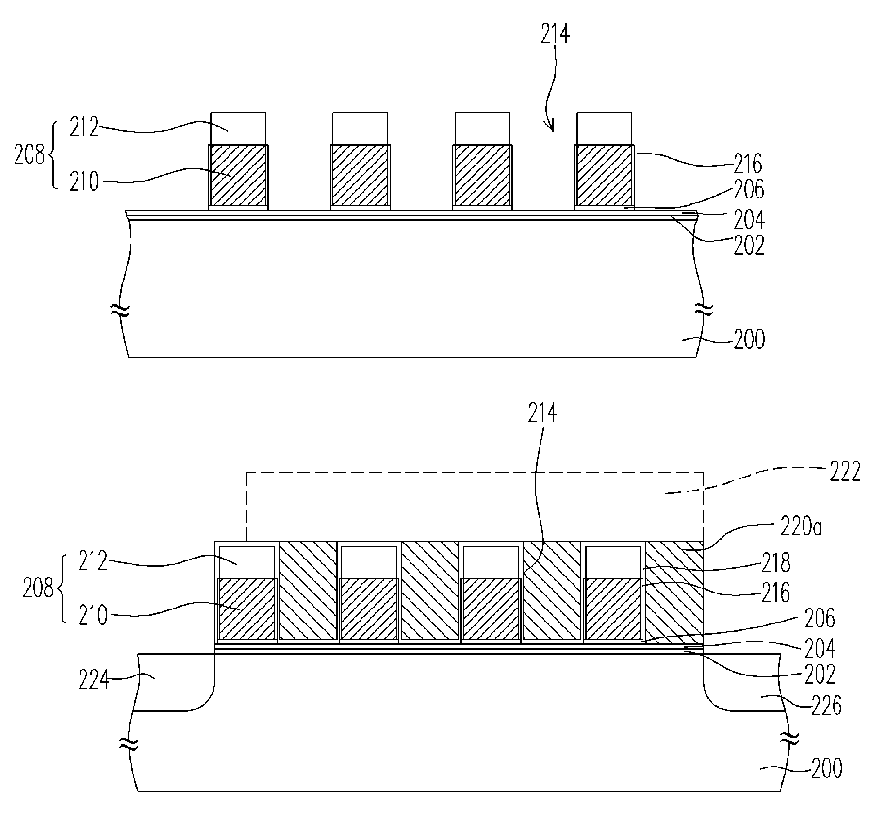
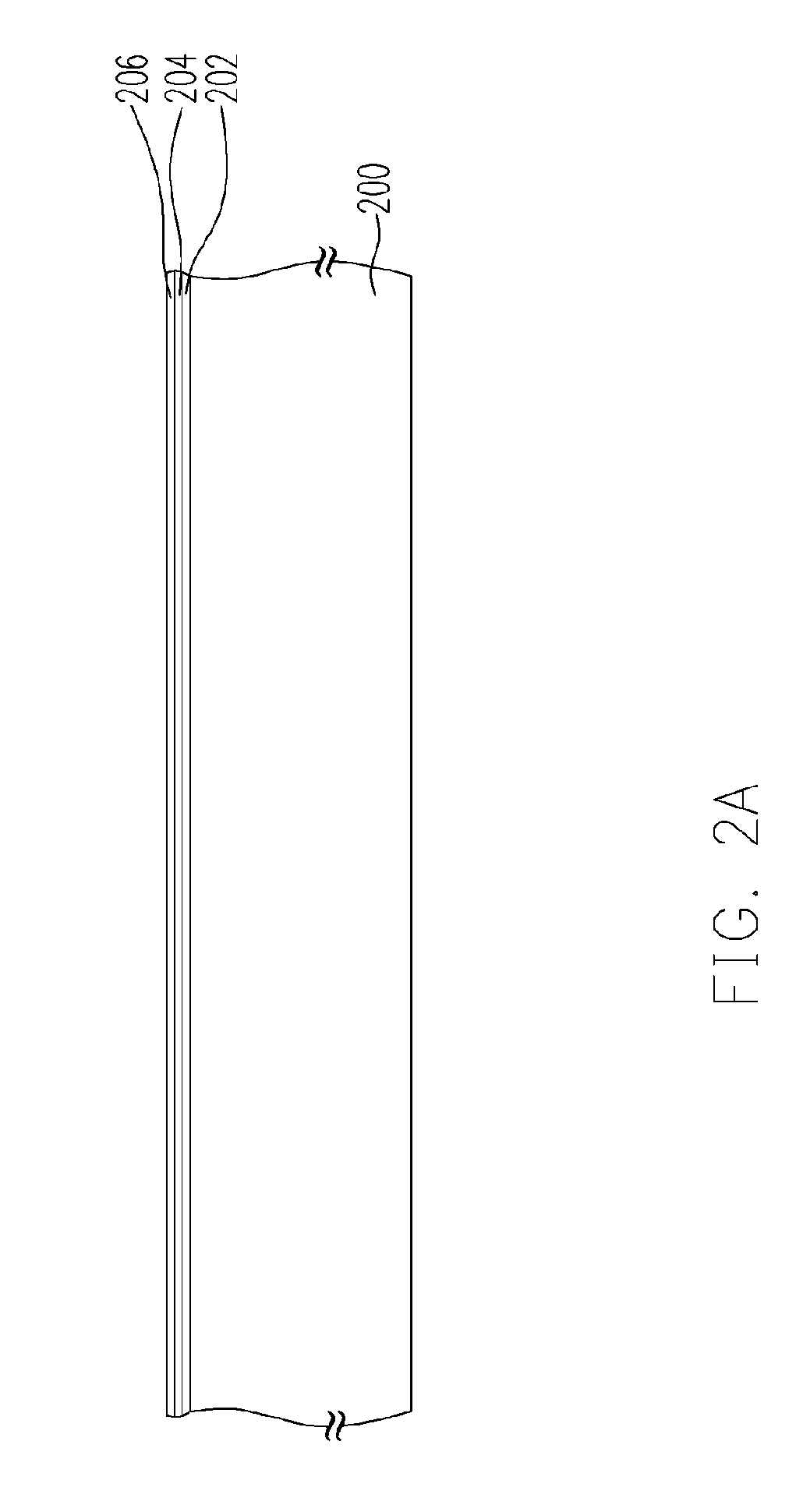
[0035]FIG. 2A to FIG. 2D are schematic cross-sectional views showing the steps for fabricating a non-volatile memory according to one embodiment of the present invention

[0036]Referring to FIG. 2A, a substrate 200 is provided, and the material for the substrate can be, for example, silicon. Then, a bottom dielectric layer 202, a charge trapping layer 204 and a top dielectric layer 206 are subsequently formed on the substrate 200. The material for the bottom dielectric layer 202 is, for example, silicon oxide, and the fabrication method can be, for example, thermal oxidation. The material for the charge trapping layer 204 is, for example, silicon nitride, and the fabrication method is, for example, chemical vapor deposition. The material for the top dielectric layer 206 is, for example, silicon oxide, and the fabrication method is, for example, chemical vapor deposition. The material for the bottom dielectric layer 202 and the top dielectric layer 206 can be other similar materials. T...


PUM


Abstract

A method of fabricating a non-volatile memory is described. A substrate is provided and a first dielectric layer, an electron trapping layer and a second dielectric layer are sequentially formed thereon. Each of the stacked gate structures includes a first gate and a cap layer having a gap between every two stacked gate structures. An oxide layer is formed on the sidewalls of the first gate. A portion of the second dielectric layer not covered by the stacked gate structures is removed. A third dielectric layer is further formed on the substrate. A second conductive layer is formed over the substrate, and a portion thereof to form second gates. The second gates and the stacked gate structures form a column of memory cells. A source region and a drain region are formed in the substrate adjacent to two sides of the column of memory cells.

Description

CROSS-REFERENCE TO RELATED APPLICATION[0001]This application claims the priority benefit of Taiwan application serial no. 94100698, filed on Jan. 11, 2005. All disclosure of the Taiwan application is incorporated herein by reference.BACKGROUND OF THE INVENTION[0002]1. Field of the Invention[0003]The present invention generally relates to a fabrication method for a semiconductor memory. More particularly, the present invention relates to a fabrication method for a non-volatile memory.[0004]2. Description of Related Art[0005]Upon various non-volatile memories, electronic erasing programming read only memory (EEPROM), which can provide the advantages of multiple data writing, reading, erasing and the data maintained even after the disconnection or the power supply, has been widely applied to the personal computers and electronic equipments.[0006]The material for the floating gate and the control gate of the conventional erasable and programmable read only memory is normally doped polys...

Claims


Application Information

Patent Timeline
IPC IPC(8): H01L21/336
CPCH01L21/28282H01L29/7923H01L29/66833H01L29/40117
Inventor PITTIKOUN, SAYSAMONE
Owner POWERCHIP SEMICON MFG CORP
Why Eureka
Try Eureka