Nonvolatile semiconductor memory device having reduced erasing time
a semiconductor memory and non-volatile technology, applied in static storage, digital storage, instruments, etc., can solve the problem of excessive supply of erase pulses, and achieve the effect of reducing erase tim
- Summary
- Abstract
- Description
- Claims
- Application Information
AI Technical Summary
Benefits of technology
Problems solved by technology
Method used
Image

Examples
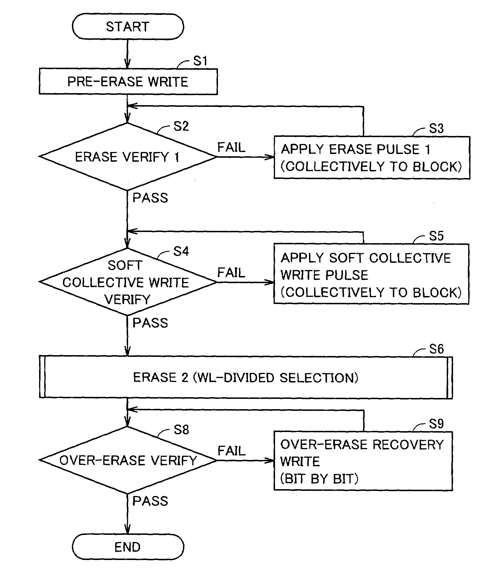
first embodiment
[0072][First Embodiment]
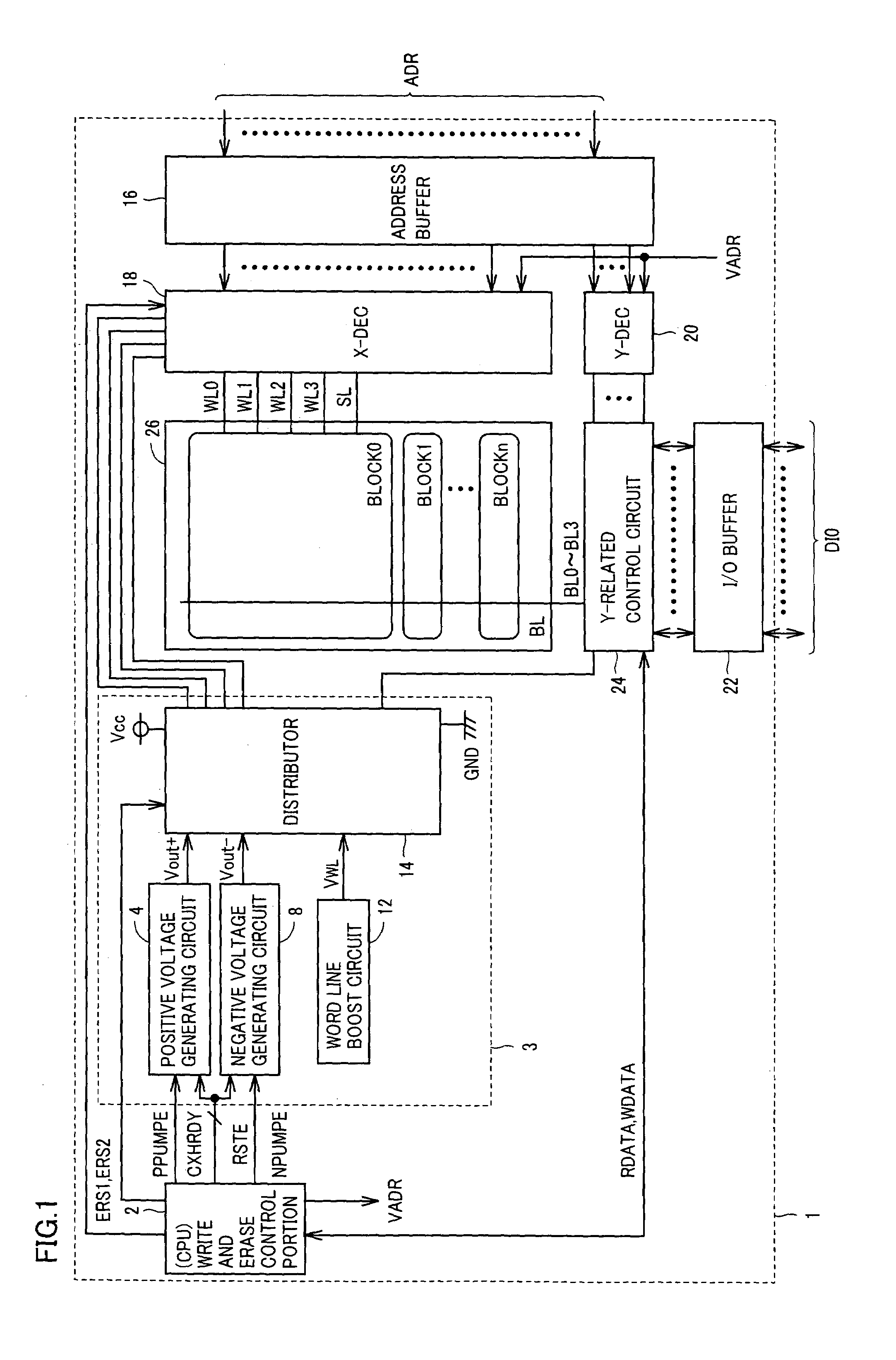
[0073]FIG. 1 is a schematic block diagram showing a structure of a nonvolatile semiconductor memory device according to a first embodiment of the invention.
[0074]Referring to FIG. 1, nonvolatile semiconductor memory device 1 includes a write and erase control portion 2, which is provided with a ROM, and controls writing and erasing according to program codes held in this ROM, a voltage generating portion 3, which receives a standby signal CXHRDY, a charge pump activating signal PPUMPE and a reset signal RSTE from write and erase control portion 2, and issues output potentials Vout+, Vout− and VWL according to these received signals, an address buffer 16 receiving an externally applied address signal ADR, an X-decoder 18, which receives an internal address signal sent from address buffer 16 and a potential supplied from voltage generating portion 3, and decides respective potentials of word lines WL0 and WL1, a source line SL and a well, an I / O buffer 22 trans...
second embodiment
[0131][Second Embodiment]
[0132]In the first embodiment, the word lines are selected for limiting the region of second application of the erase pulse. Instead of selecting the word lines, the second embodiment uses the bit lines for limiting the region of application of the erase pulse.
[0133]A nonvolatile semiconductor memory device of the second embodiment includes an X-decoder 18A instead of X-decoder 18 in the structure shown in FIG. 1, and write and erase control portion 2 performs the control by applying signals ERS to X-decoder 18A in a manner different from that of the first embodiment.
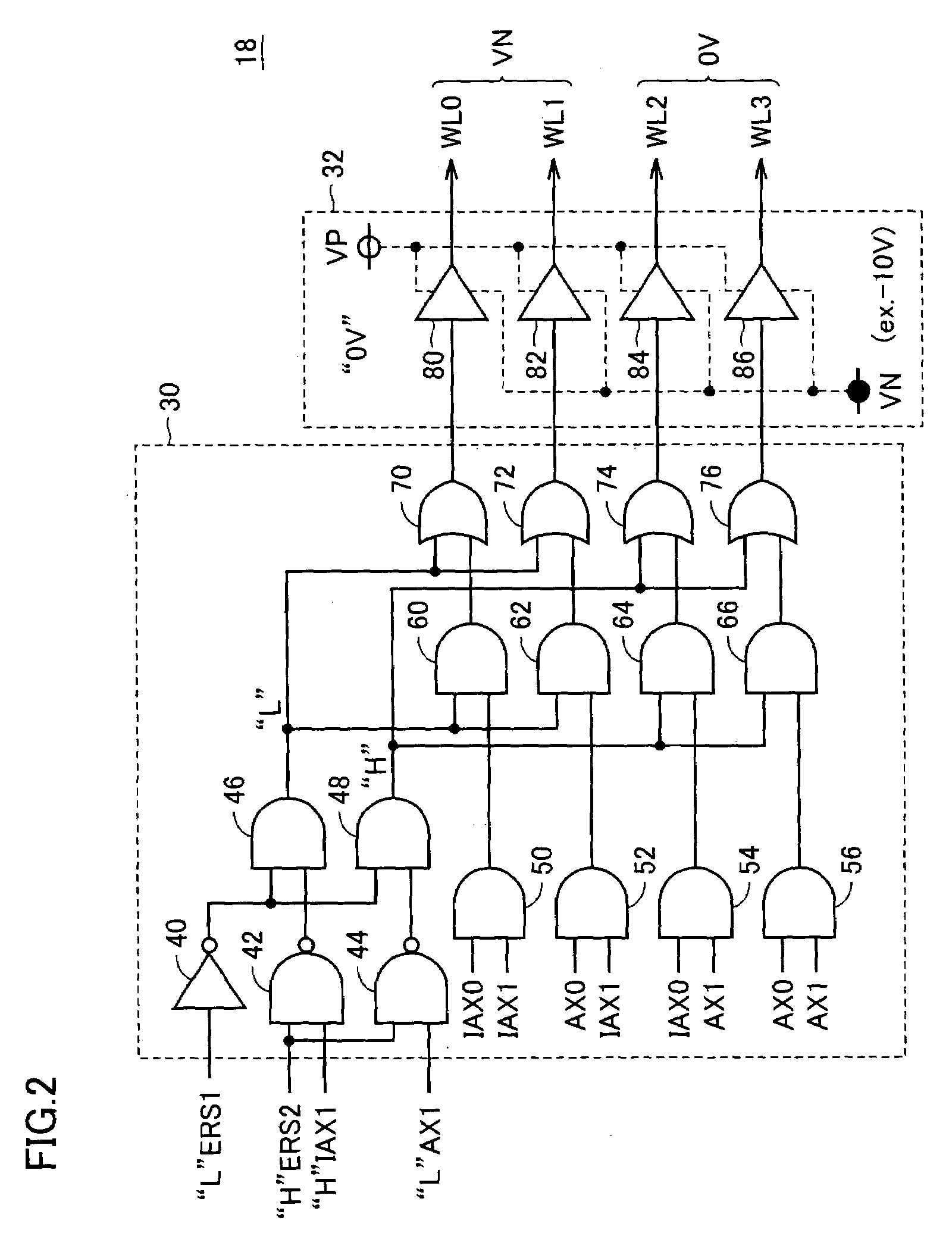
[0134]FIG. 6 is a circuit diagram showing a structure of X-decoder 18A used in the second embodiment.
[0135]Referring to FIG. 6, X-decoder 18A includes a select portion 30A instead of select portion 30 in the structure of X-decoder 18 shown in FIG. 2.
[0136]Select portion 30A includes an inverter 98 receiving and inverting signal ERS, an AND circuit 100 receiving signals IAX0 and IAX1, an AND circ...
third embodiment
[0155][Third Embodiment]
[0156]For applying the erase pulse, the number of word lines to be selected is restricted in the first embodiment, and the number of bit lines to be selected is restricted in the second embodiment. In a third embodiment, these manners are combined, and both the number of the bit lines to be selected and the number of the bit lines to be selected are restricted for applying the erase pulse.
[0157]Referring to FIG. 11, the operation of block erasing in the third embodiment includes a step S20 instead of step S6 in the flow of block erasing of the first embodiment illustrated in FIG. 4. In step S20, the word lines and the bit lines are divided into multiple groups for selection.
[0158]More specifically, X-decoder 18 shown in FIG. 2 is used, and the setting data of the bit lines to be applied from write and erase control portion 2 to Y-related control circuit 24 is limited corresponding to the address, which is being verified.
[0159]FIG. 12 is a flowchart for illust...
PUM
 Abstract
Description
Claims
Application Information
 - R&D
- Intellectual Property
- Life Sciences
- Materials
- Tech Scout
- Unparalleled Data Quality
- Higher Quality Content
- 60% Fewer Hallucinations
Browse by: Latest US Patents, China's latest patents, Technical Efficacy Thesaurus, Application Domain, Technology Topic, Popular Technical Reports.
© 2025 PatSnap. All rights reserved.Legal|Privacy policy|Modern Slavery Act Transparency Statement|Sitemap|About US| Contact US: help@patsnap.com