Split gate type nonvolatile semiconductor memory device, and method of fabricating the same

a semiconductor memory and nonvolatile technology, applied in the direction of semiconductor devices, electrical devices, transistors, etc., can solve problems such as overlap variation

Inactive Publication Date: 2006-04-18
SAMSUNG ELECTRONICS CO LTD
View PDF6 Cites 3 Cited by
  • Summary
  • Abstract
  • Description
  • Claims
  • Application Information

AI Technical Summary

Benefits of technology

[0011]The present invention provides a split gate type nonvolatile semiconductor memory device, and a method of fabricating the same, in which a floating gate and a control gate are formed in a self-alignment approach such that an effective channel length is identically provided between adjacent memory cells to overcome an on-cell difference in characteristics between an odd cell and an even cell.
[0012]Also, the present invention provides a split gate type nonvolatile semiconductor memory device, and a method of fabricating the same, in which an overlap of a floating gate and a control gate can be flexibly controlled.

Problems solved by technology

However, the photolithography process can cause misalignment, thereby causing an overlap variation.

Method used


Image

  • Split gate type nonvolatile semiconductor memory device, and method of fabricating the same
  • Split gate type nonvolatile semiconductor memory device, and method of fabricating the same
  • Split gate type nonvolatile semiconductor memory device, and method of fabricating the same

Examples


Embodiment Construction

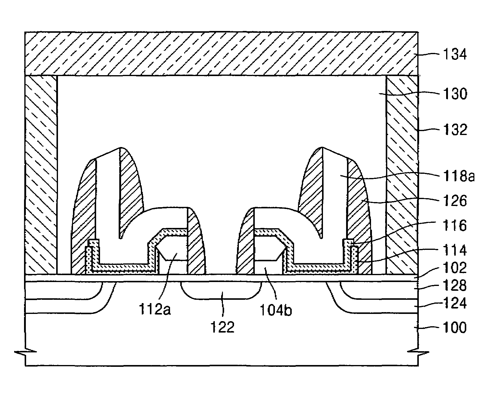
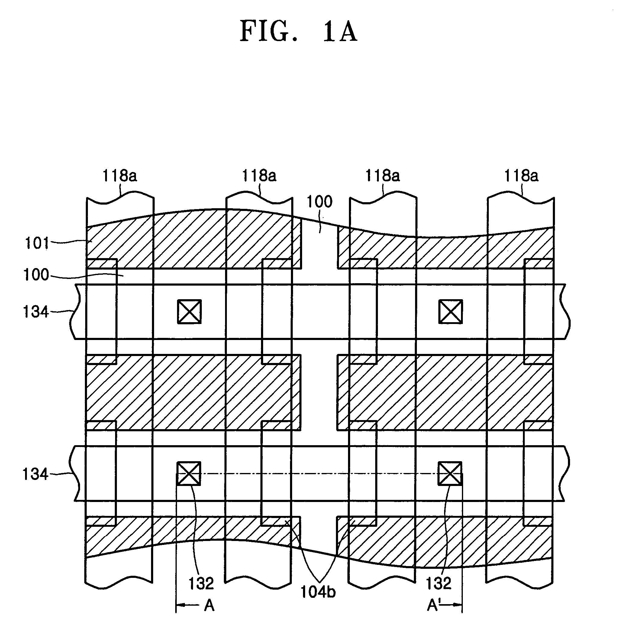
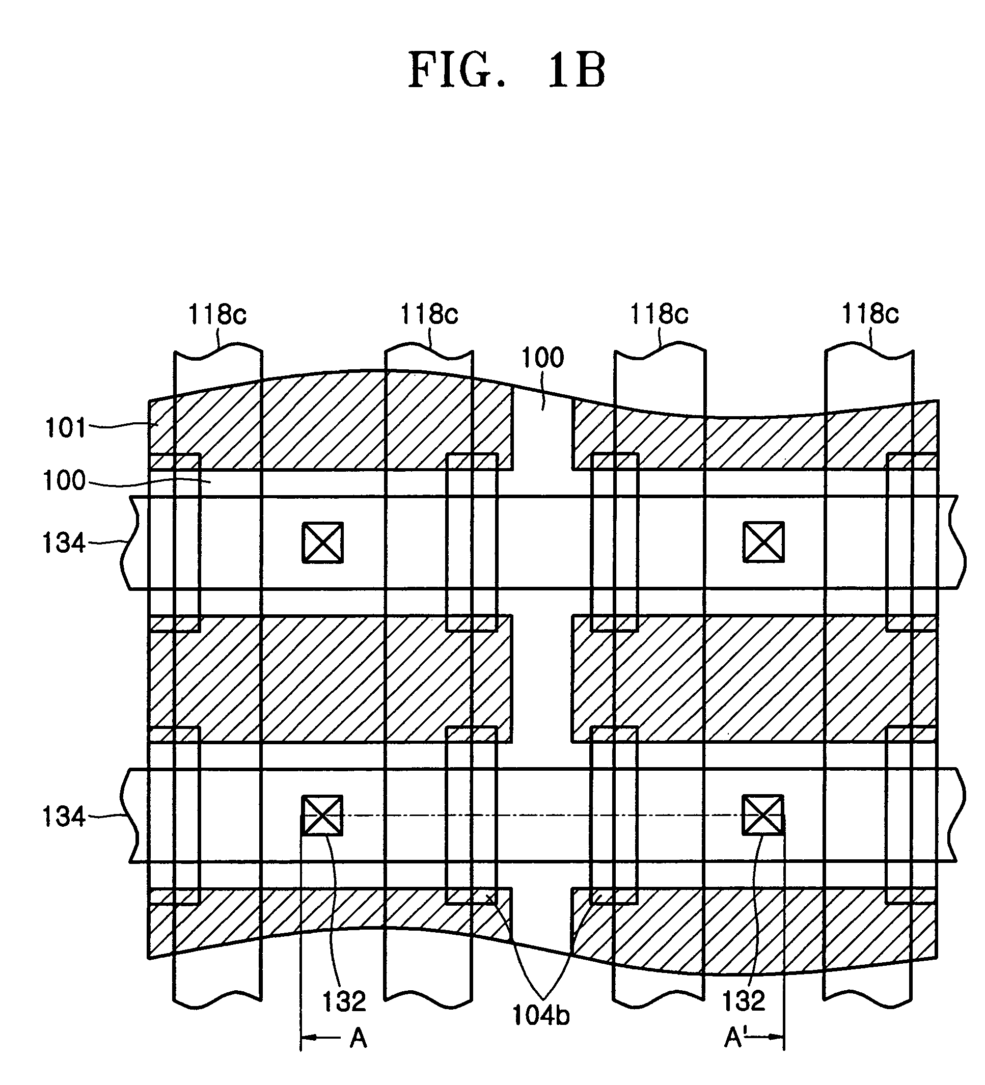
[0030]FIGS. 1A and 1B are schematic layouts illustrating main structural elements of a split gate type nonvolatile semiconductor memory device according to embodiments of the present invention. FIG. 12 is a sectional view illustrating the split gate type nonvolatile semiconductor memory device taken along line A–A′ of FIG. 1A, and FIG. 20 is a sectional view illustrating the split gate type nonvolatile semiconductor memory device taken along line A–A′ of FIG. 1B. A first embodiment of the invention shown in FIGS. 1A and 2 through 12 is different from the second embodiment of the present invention shown in FIGS. 1B and 13 through 20 in that, in the first embodiment of FIGS. 1A and 2 through 12, the floating gate 104b is completely or almost completely overlapped by the control gate 118a, and, in the second embodiment of FIGS. 1B and 13 through 20, the floating gate 104b is only partially overlapped by the control gate 118c.

[0031]Referring to FIGS. 1A, 1B 12 and 20, a device isolatio...


PUM


Abstract

A split gate type nonvolatile semiconductor memory device and a method of fabricating a split gate type nonvolatile semiconductor memory device are provided. A gate insulating layer and a floating-gate conductive layer are formed on a semiconductor substrate. A mask layer pattern is formed on the floating-gate conductive layer to define a first opening extending in a first direction. First sacrificial spacers having a predetermined width are formed on both sidewalls corresponding to the mask layer pattern. An inter-gate insulating layer is formed on the floating-gate conductive layer. The first sacrificial spacers are removed, and the floating-gate conductive layer is etched until the gate insulating layer is exposed. A tunneling insulating layer is formed on an exposed portion of the floating-gate conductive layer. A control-gate conductive layer is formed on a surface of the semiconductor substrate. Second sacrificial spacers having predetermined widths are formed on the control-gate conductive layer. A split control gate is formed in the first opening, by etching the exposed control-gate conductive layer. The remaining mask layer pattern and inter-gate insulating layer are etched until the floating-gate conductive layer is exposed. The exposed floating-gate conductive layer is etched to form a split floating gate in the first opening.

Description

[0001]This application claims the priority of Korean Patent Application No. 2004-18289, filed on Mar. 18, 2004, in the Korean Intellectual Property Office, the contents of which are incorporated herein in their entirety by reference.BACKGROUND OF THE INVENTION[0002]1. Field of the Invention[0003]The present invention relates to a split gate type nonvolatile semiconductor memory device, and a method of fabricating the same, and more particularly, to a split gate type nonvolatile semiconductor memory device using a self-alignment approach to overcome misalignment of a control gate, and a method of fabricating the same.[0004]2. Description of the Related Art[0005]The applications for nonvolatile semiconductor memory devices have been increasing in various fields such as mobile communication systems, memory cards and the like, since it can electrically erase and store and retain data even when power is not applied. Among nonvolatile semiconductor memories, a flash memory can program in ...

Claims


Application Information

Patent Timeline
Patent Type & Authority Patents(United States)
IPC IPC(8): H01L21/336H01L21/8247H01L21/28H01L27/115H01L29/423H01L29/51H01L29/788H01L29/792
CPCH01L21/28273H01L27/115H01L29/7881H01L29/42324H01L29/513H01L27/11521H01L29/40114H10B69/00H10B41/30
Inventor JEON, HEESEOGYOON, SEUNG-BEOMKIM, YONG-TAECHOI, YONG-SUK
Owner SAMSUNG ELECTRONICS CO LTD
Why Eureka
Try Eureka