Capacitive load driving circuit driving capacitive loads such as pixels in plasma display panels and plasma display apparatus having the capacitive load driving circuit
- Summary
- Abstract
- Description
- Claims
- Application Information
AI Technical Summary
Benefits of technology
Problems solved by technology
Method used
Image
Examples
first embodiment
[0086]FIG. 11 is a block circuit diagram showing a capacitive load driving circuit according to the present invention.
[0087]As is apparent from a comparison between FIG. 11 and FIG. 5, the capacitive load driving circuit of the first embodiment corresponds to a circuit in which the delay circuits 51 to 54 in the prior art sustain circuit (capacitive load driving circuit) shown in FIG. 5 are constructed from front-edge delay circuits 61 to 64 and back-edge delay circuits 71 to 74, respectively. Accordingly, the driving operation of the drive capacitor Cp by the switch devices (sustain output devices: n-channel MOS transistors) 31 and 33 and amplifiers (drive circuits) 32 and 34, the operation of the power recovery circuit by the switch devices 37 and 40, amplifying circuits 38 and 41, diodes 36 and 42, inductances 35 and 43, and capacitor 39 (Cp), etc. are the same as those described in detail with reference to FIG. 5, and the description will not be repeated there.
[0088]As shown in ...
second embodiment
[0090]FIG. 12 is a block circuit diagram showing a capacitive load driving circuit according to the present invention.
[0091]As is apparent from a comparison between FIG. 12 and FIG. 11, the capacitive load driving circuit of the second embodiment is a circuit in which the front-edge delay circuits 61 to 64 and the back-edge delay circuits 71 to 74 in the capacitive load driving circuit of the first embodiment are constructed respectively as rising edge delay circuits 611 to 641 for delaying the rising edges of the respective input signals V1 to V4 and falling edge delay circuits 711 to 741 for delaying the falling edges of the respective input signals V1 to V4. Here, the input signals V1 to V4 are each a positive polarity pulse signal (high enable signal) which is active at a high level “H”.
third embodiment
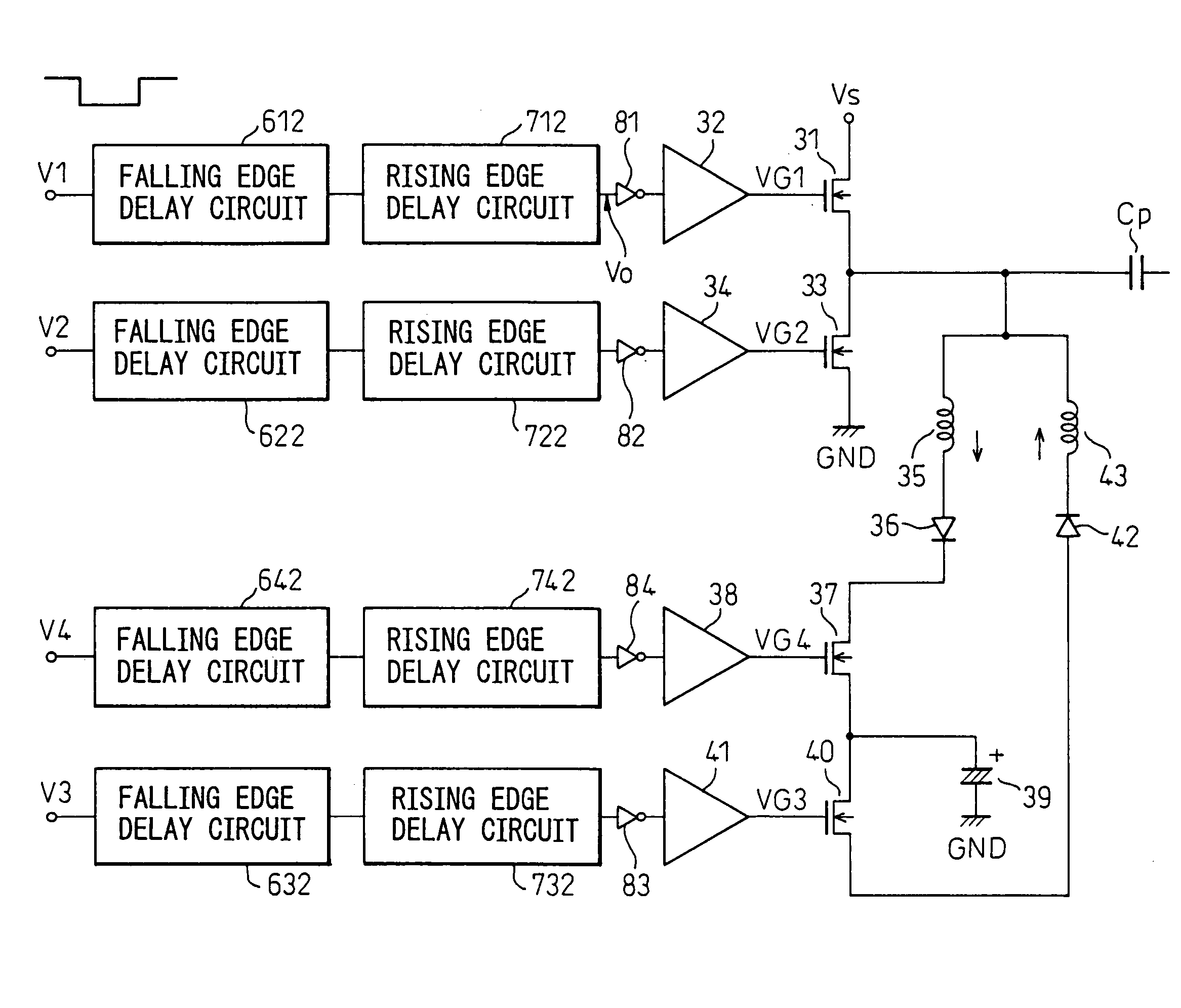
[0092]FIG. 13 is a block circuit diagram showing a capacitive load driving circuit according to the present invention.
[0093]As is apparent from a comparison between FIG. 13 and FIG. 11, the capacitive load driving circuit of the third embodiment is a circuit in which the front-edge delay circuits 61 to 64 and the back-edge delay circuits 71 to 74 in the capacitive load driving circuit of the first embodiment are constructed respectively as falling edge delay circuits 612 to 642 for delaying the falling edges of the respective input signals V1 to V4 and rising edge delay circuits 712 to 742 for delaying the rising edges of the respective input signals V1 to V4. Here, the input signals V1 to V4 are each a negative polarity pulse signal (low enable signal) which is active at a low level “L”. Output signals from the rising edge delay circuits 712 to 742 are supplied to the corresponding switch devices (31, 33, 40, and 37) via inverters 81 to 84, respectively.
[0094]FIG. 14 is a circuit d...
PUM
 Abstract
Description
Claims
Application Information
 - R&D
- Intellectual Property
- Life Sciences
- Materials
- Tech Scout
- Unparalleled Data Quality
- Higher Quality Content
- 60% Fewer Hallucinations
Browse by: Latest US Patents, China's latest patents, Technical Efficacy Thesaurus, Application Domain, Technology Topic, Popular Technical Reports.
© 2025 PatSnap. All rights reserved.Legal|Privacy policy|Modern Slavery Act Transparency Statement|Sitemap|About US| Contact US: help@patsnap.com


