
Self-adjusting programmable on-chip clock aligner

Active Publication Date: 2006-03-21
CISCO TECH INC
View PDF9 Cites 13 Cited by
  • Summary
  • Abstract
  • Description
  • Claims
  • Application Information

AI Technical Summary

Problems solved by technology

However, the use of extra wire reduces the quality of the clock signal and consumes already limited space on the printed circuit board.
However, in addition to reliability and stability concerns, PLLs commonly require the use of a dedicated constantly running input clock signal, which may not be available, or which may not be cost effective to implement.
The use of on-chip delays, such as a PLL, suffers from another disadvantage in that they are susceptible to operating conditions.
The precision by which a signal can be delayed, inside an integrated circuit for example, is limited by environmental and manufacturing conditions.
Because integrated circuits are expected to operate over a range of temperatures and voltages, the transistors themselves are unable to provide a constant delay when environmental conditions vary.

Method used


Image

  • Self-adjusting programmable on-chip clock aligner
  • Self-adjusting programmable on-chip clock aligner
  • Self-adjusting programmable on-chip clock aligner

Examples


Embodiment Construction

Introduction

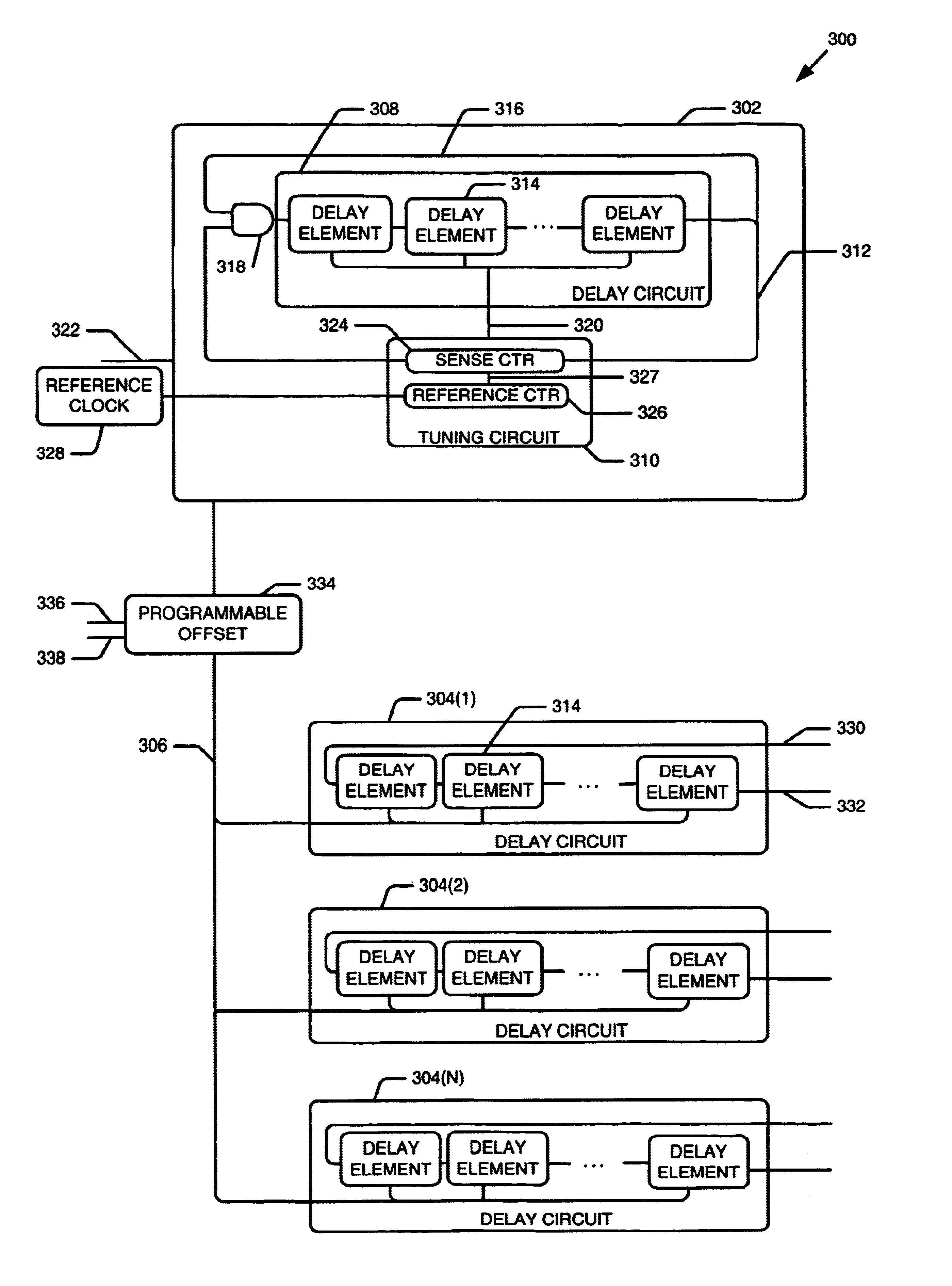
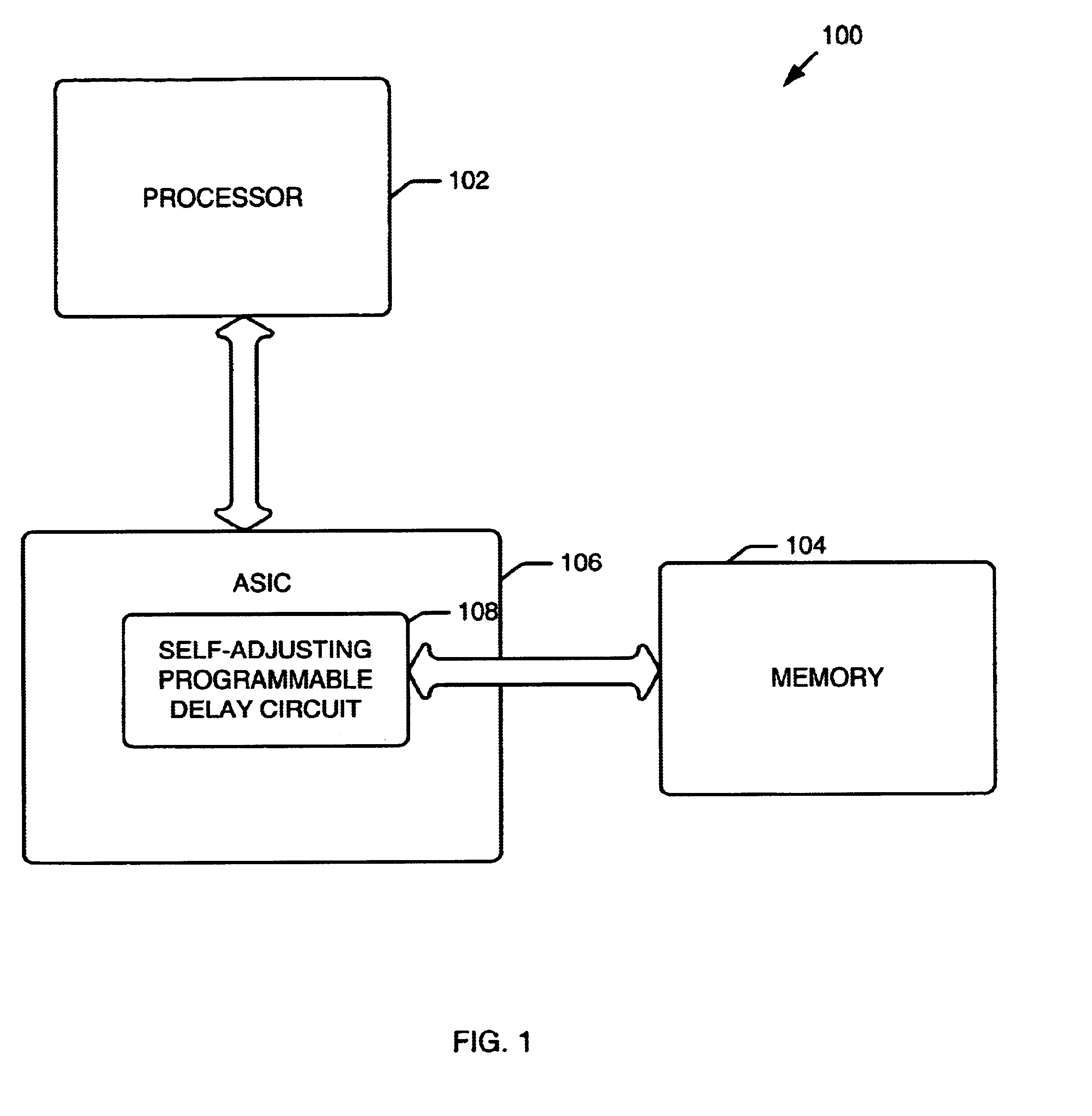
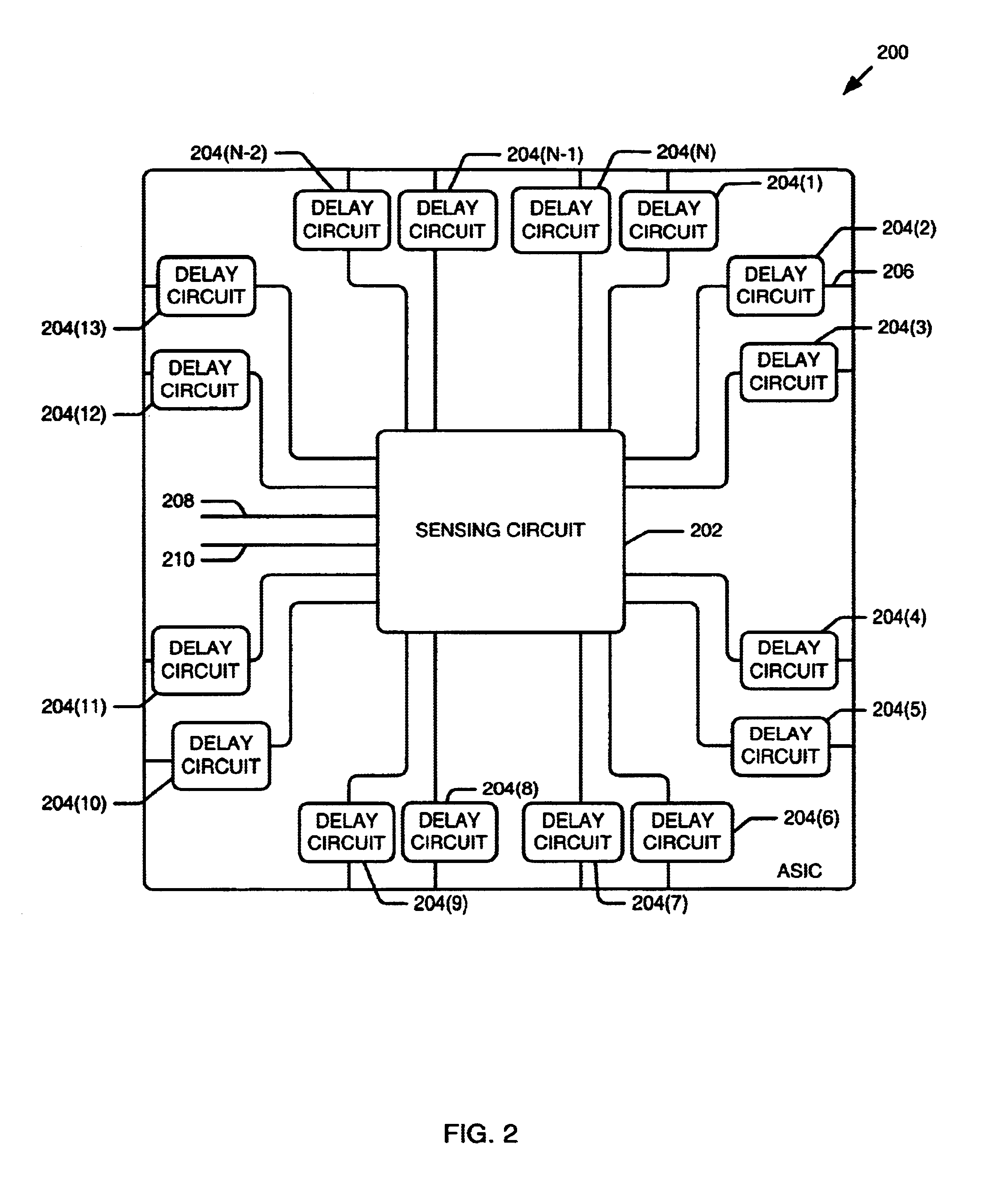
[0017]The present invention generally provides a self-adjusting programmable delay circuit that is able to provide a signal delay independent of process, voltage, and temperature (PVT) variations. In one embodiment of the present invention, a sensing circuit and a number of delay elements are provided on an integrated circuit. In response to receiving a programmed delay, the sensing circuit, coupled to a free-running clock, is configured to repeatedly determine a delay element length to satisfy the programmed delay and provide the determined delay element length to the delay circuits. The delay circuits are configured to provide a delayed signal having a delay which also satisfies the programmed delay and which is independent of (i.e., substantially unaffected by) process, temperature, and voltage (PVT) variations.

[0018]Embodiments of the present invention provide the ability to program a delay, and also provide a delayed signal having a delay satisfying the programmed d...


PUM


Abstract

A circuit including a sensing circuit, which includes a first delay circuit and a tuning circuit. The tuning circuit includes a sense counter and a reference counter. The sense counter is coupled to the first delay circuit and is configured to count a number of oscillations provided by the first delay circuit and provide a notification to the tuning circuit when the sense counter reaches a threshold value. The reference counter is coupled to the sense counter and a reference clock. The reference counter is configured to store a reference time which represents a time elapsed for the sense counter to reach the threshold value. Also included in the circuit is a second delay circuit coupled to the sensing circuit.

Description

BACKGROUND OF THE INVENTION[0001]1. Field of the Invention[0002]The present invention relates generally to interface circuits, and more specifically, to circuits that provide a programmable time delay substantially unaffected by process, voltage, and temperature variations.[0003]2. Description of the Related Art[0004]Interfacing with many source synchronous circuits (e.g., DRAM memories, and variations thereof) requires precise signal timing. For example, interfacing to DDR DRAM memories requires a clock signal and one or more data signals to be preferably adjusted so that the clock signal arrives at the DDR DRAM memory in the middle of a data valid window.[0005]Traditionally, the time adjustment of clock signals has been accomplished by increasing the length of the clock line on the printed circuit board until the optimal timing is achieved. However, the use of extra wire reduces the quality of the clock signal and consumes already limited space on the printed circuit board. Anothe...

Claims


Application Information

Patent Timeline
IPC IPC(8): H03H11/26G01R31/317G06F1/04G11C29/02H03L7/081H03L7/099
CPCG01R31/31725G06F1/04G11C29/02H03L7/0997G11C29/50012H03L7/0805H03L7/0812G11C29/028
Inventor FEINBERG, EUGENE M.PAUL, RICHARD F.MANELA, PHILIP R.
Owner CISCO TECH INC
Learn More