Semiconductor device with reduced interconnection capacity

a technology of nitride film and interconnection capacity, which is applied in the direction of semiconductor devices, semiconductor/solid-state device details, electrical apparatus, etc., can solve the problems of high dielectric constant of /b>, high stress, and inability to speed up small devices, etc., to achieve low interconnection capacity and reduce stress placed on nitride film

Inactive Publication Date: 2006-03-21
LAPIS SEMICON CO LTD
View PDF17 Cites 4 Cited by
  • Summary
  • Abstract
  • Description
  • Claims
  • Application Information

AI Technical Summary

Benefits of technology

[0013]This structure allows the nitride film pattern to be formed with a shape and size that encloses the perimeter of the bottom of the wiring groove. If, in the configuration of the semiconductor device, a plurality of structures with wiring grooves and holes are provided separately, the nitride film pattern is formed with a size and shape that prevents neighbouring nitride film patterns from coming into contact with one another. That is, the perimeter of the nitride film pattern is only slightly larger than the size of the bottom of the wiring groove and therefore much smaller than the total area of the base oxide film. Therefore, the stress placed on the nitride film can be reduced and a semiconductor device made with a low interconnection capacity.

Problems solved by technology

However, attempts to speed up smaller devices are hampered by line delays.
It is difficult to use the dry etching process used when forming Al line on Cu film (or layer) when forming the Cu line.
However, the nitride film 104x used as the etching mask used for the base oxide film 102 is generally known to have a high dielectric constant and be highly subject to stress.
This causes problems such as cracks in the nitride film or deformation of the hole pattern formed in the nitride film.
Also, the thicker the nitride film, the greater the interconnection capacity, the cause of line delays.

Method used


Image

  • Semiconductor device with reduced interconnection capacity
  • Semiconductor device with reduced interconnection capacity
  • Semiconductor device with reduced interconnection capacity

Examples


first embodiment

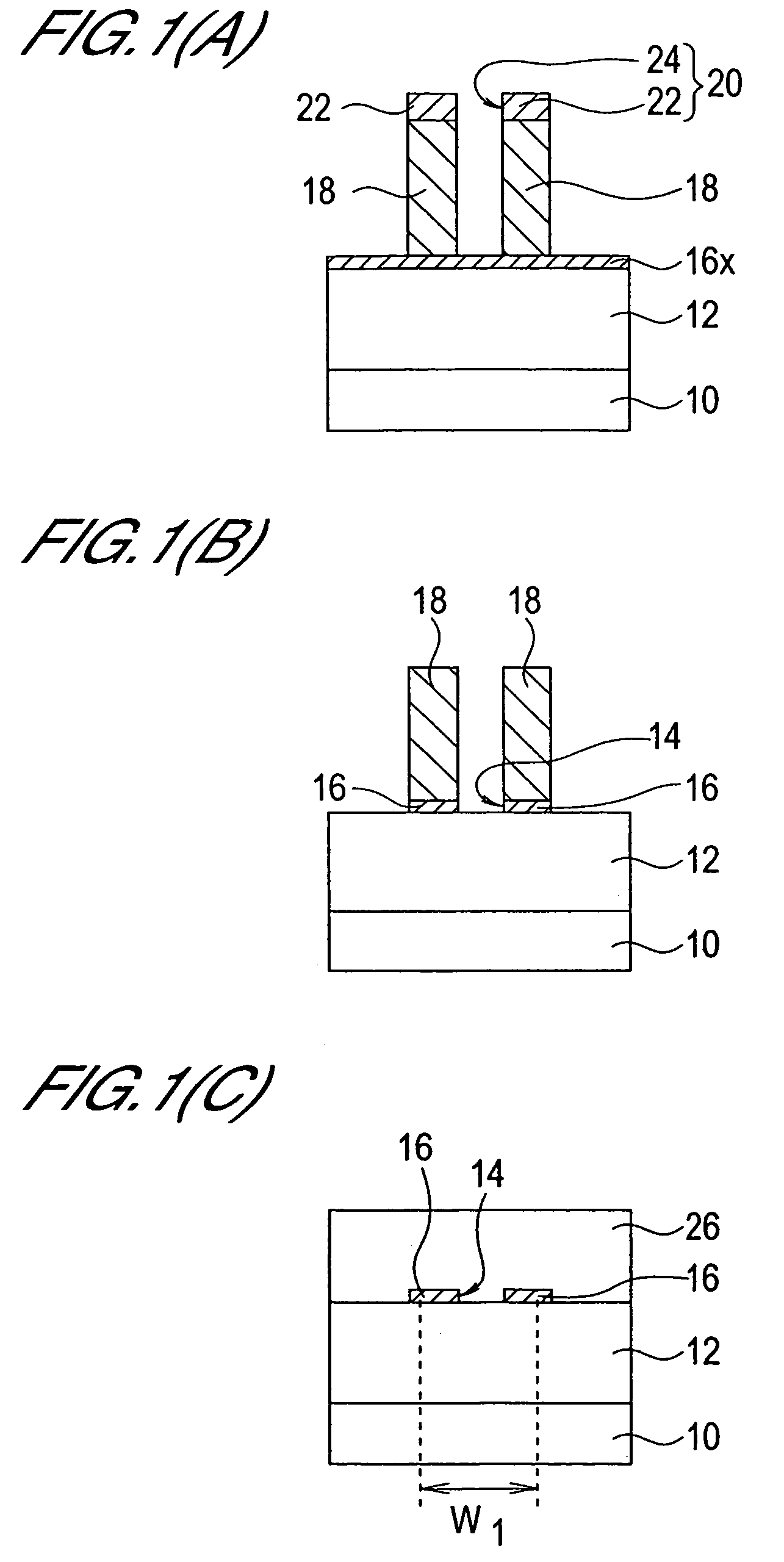
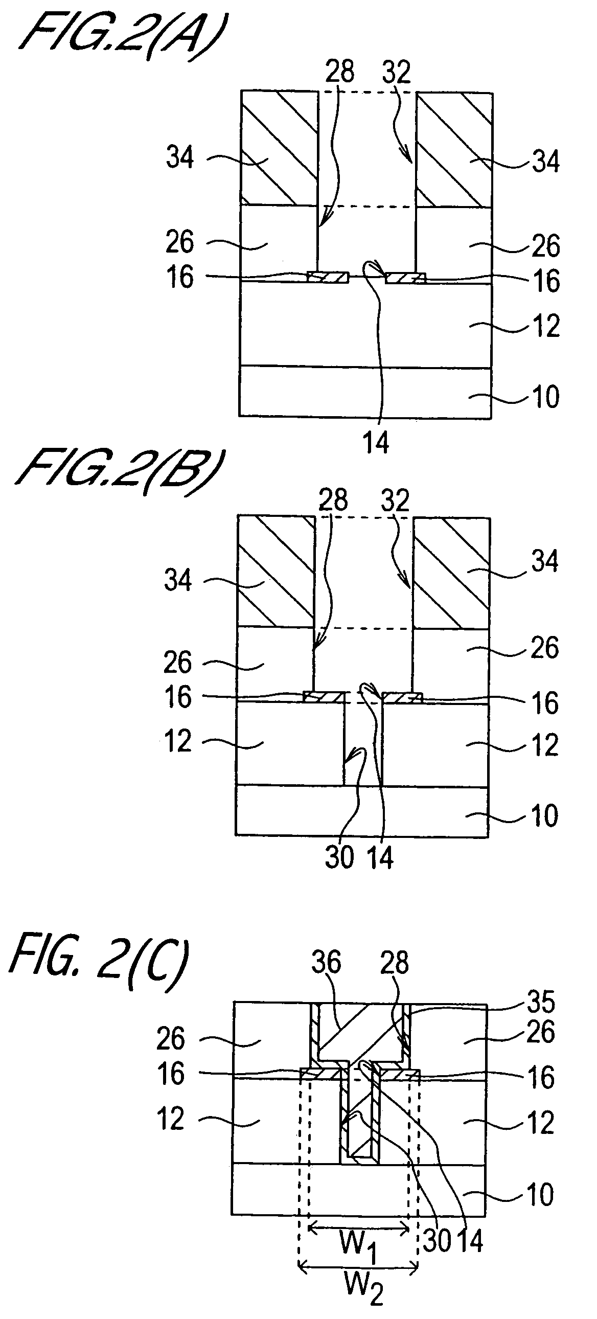
[0043]With reference to FIGS. 1 through 4, an example of the manufacture of a semiconductor using the dual damascene process will be explained as a first embodiment of the present invention.

[0044]FIGS. 1 to 3 give overviews of the processes involved in the manufacture of semiconductor devices in the embodiment of the present invention. They provide cross sections taken at positions on the structure during manufacture that have both a hole for a contact between lines and a groove for a line. FIG. 4 is a general schematic view of the mask used in photo lithography processing.

[0045]Firstly, a base oxide film 12 as a lower oxide film is formed on a underlayer 10 (process 1-1) (FIG. 1(A)).

[0046]In this example, the CVD method is used to form an SiO2 film, which is the base oxide film 12, of between 500 and 800 nm in depth on the Si substrate 10 used as the underlayer.

[0047]Next, a nitride film pattern 16 with a hole pattern 14 is formed on the base oxide film 12 (process 1-2) (FIGS. 1(A)...

second embodiment

[0062]With reference to FIGS. 5, 6 and 7, an example of the formation of a nitride film pattern using a method different to that used in the first embodiment will be explained as a second embodiment of the present invention.

[0063]FIGS. 5 and 6 provide overviews of the processes involved in the manufacture of the semiconductor devices of this embodiment of the present invention. They provide cross sections taken at positions on the structure during manufacture that have both a hole for the contact between lines and a groove for line.

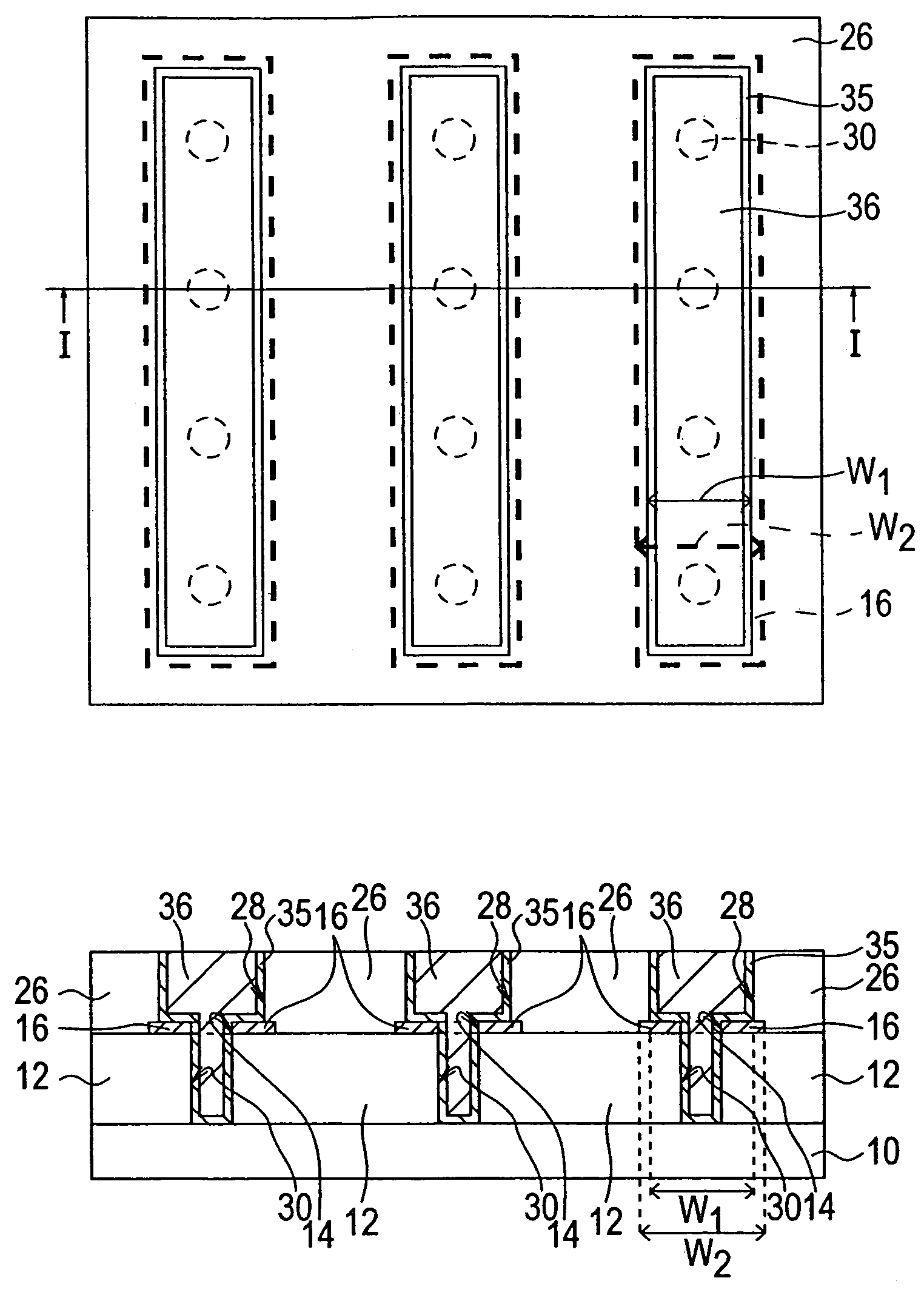
[0064]FIGS. 7(A) and 7(B) show a partial plan view of a semiconductor device of the second embodiment of the present invention and a cross-sectional view taken along the line I—I of FIG. 7(A), respectively.

[0065]Below, those points that differ from the first embodiment will be explained and detailed explanation of those points that are the same, as the first embodiment will be omitted.

[0066]Firstly, the base oxide film 12 is formed on the substrate 10 (pr...

third embodiment

[0080]With reference to FIGS. 8, 9 and 10, an example of the formation of a nitride film pattern using a method different to that used in either the first or second embodiment will be explained as a third embodiment of the present invention.

[0081]FIGS. 8 and 9 provide overviews of the processes involved in the manufacture of the semiconductor devices of this embodiment of the present invention. They provide cross sections taken at positions on the structure during manufacture that have both a hole for the contact between lines and a groove for line.

[0082]FIGS. 10(A) and 10(B) show a partial plan view of a semiconductor device of the third embodiment of the present invention and a cross-sectional view taken along the line I—I of FIG. 10(A), respectively.

[0083]Below, those points that differ from the first and second embodiments will be explained and detailed explanation of those points that are the same as the first and second embodiments will be omitted.

[0084]Firstly, the base oxide...


PUM


Abstract

This invention provides a semiconductor device that can ensure that stress on the nitride film is not increased or is reduced, and that can prevent an increase in interconnection capacity. The semiconductor device comprises a underlayer, a base oxide film that is formed on this underlayer, a nitride film pattern with a hole pattern that is provided on this base oxide film, holes that penetrate the base oxide film, an upper oxide film provided on the base oxide film to cover the nitride film pattern, wiring grooves provided through the upper oxide film in which part of the nitride film pattern including the hole pattern is exposed, and wiring metal that fills the holes and wiring grooves. The nitride film pattern is formed with such a shape and size that surrounds the outside of the wiring grooves and is separate from neighbouring nitride film patterns.

Description

[0001]This nonprovisional application is a divisional of U.S. application Ser. No. 09 / 736,140, filed Dec. 15, 2000 now U.S. Pat. No 6,825,566.BACKGROUND OF THE INVENTION[0002]1. Field of the Invention[0003]The present invention relates to a semiconductor device structure and its manufacturing method, and more particularly to a manufacturing method for a semiconductor device that uses a dual damascene process in which a metal material is embedded into both a wiring groove and a hole used for the contact between lines.[0004]2. Description of Related Art[0005]Recent years have seen the need for acceleration of semiconductor devices such as LSIs and a trend towards much smaller devices. However, attempts to speed up smaller devices are hampered by line delays. Use of low resist Cu line instead of the conventional Al line is proposed to solve this problem of line delays.[0006]It is difficult to use the dry etching process used when forming Al line on Cu film (or layer) when forming the C...

Claims


Application Information

Patent Timeline
Patent Type & Authority Patents(United States)
IPC IPC(8): H01L21/4763H01L21/302H01L21/306H01L21/3065H01L21/768H01L23/48H01L23/522
CPCH01L21/76801H01L21/7681H01L21/76829H01L23/5222H01L23/5226H01L21/76804H01L21/76841H01L21/76843H01L2924/0002H01L2924/00
Inventor SAKATA, TOYOKAZUINUI, HIDENORI
Owner LAPIS SEMICON CO LTD
Why Eureka
Try Eureka