Gain-clamped semiconductor optical amplifier using Raman amplification principle

Inactive Publication Date: 2006-03-14
SAMSUNG ELECTRONICS CO LTD
View PDF6 Cites 9 Cited by
  • Summary
  • Abstract
  • Description
  • Claims
  • Application Information

AI Technical Summary

Benefits of technology

[0018]Accordingly, the present invention has been made to solve at least the above-mentioned problems occurring in the prior art. The present invention provides a gain-clamped semiconductor optical amplifier using Raman amplification principle in which the gain-clamped semiconductor optical amplifier has high gain characteristics and a low noise figure, without additional pumping light source for a Raman amplifier.

Problems solved by technology

If the case is such that a signal arriving at the receiver has a power reduced below a threshold value, it may be impossible to perform a normal optical communication because of a receiving errors.
In addition, the use of optical amplifiers dramatically increases the transmission distance without optical electrical conversion.
However, the EDFA has drawbacks in that the costs associated with this particular amplifier is high.
Moreover, the operational wavelength of an EDFA is limited to the 1.5 μm band.
However, as shown in FIG. 2, the gain-clamped semiconductor optical amplifier also has a very high noise figure, up to 8 dB, thereby having a limit in application in a metropolitan area or access area.
The Raman amplifier also has drawbacks in that not only does this type of amplifier have a very low optical amplification efficiency, but the Raman amplifier also needs a high-priced pumping light source.
In addition to the increased costs introduced by requiring a high-priced pumping light source, there is a problem with regard to that of size, as the whole optical amplifier module size is increased.
Accordingly, the use of the laser pump makes it very difficult to reduce the size of the optical amplifier and to produce low-cost optical amplifiers.
Furthermore, as the conventional optical amplifier drives two active elements, there is an additional disadvantage in that the power consumption is large.

Method used


Image

  • Gain-clamped semiconductor optical amplifier using Raman amplification principle
  • Gain-clamped semiconductor optical amplifier using Raman amplification principle
  • Gain-clamped semiconductor optical amplifier using Raman amplification principle

Examples


Embodiment Construction

[0033]Hereinafter, a gain-clamped semiconductor optical amplifier using the Raman amplification principle according to preferred embodiments of the present invention will be described with reference to the accompanying drawings. It is to be noted that the same elements are indicated with the same reference numerals throughout the drawings. For the purposes of clarity and simplicity a detailed description of known functions and configurations incorporated herein will be omitted as it may make the subject matter of the present invention unclear.

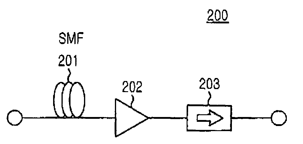
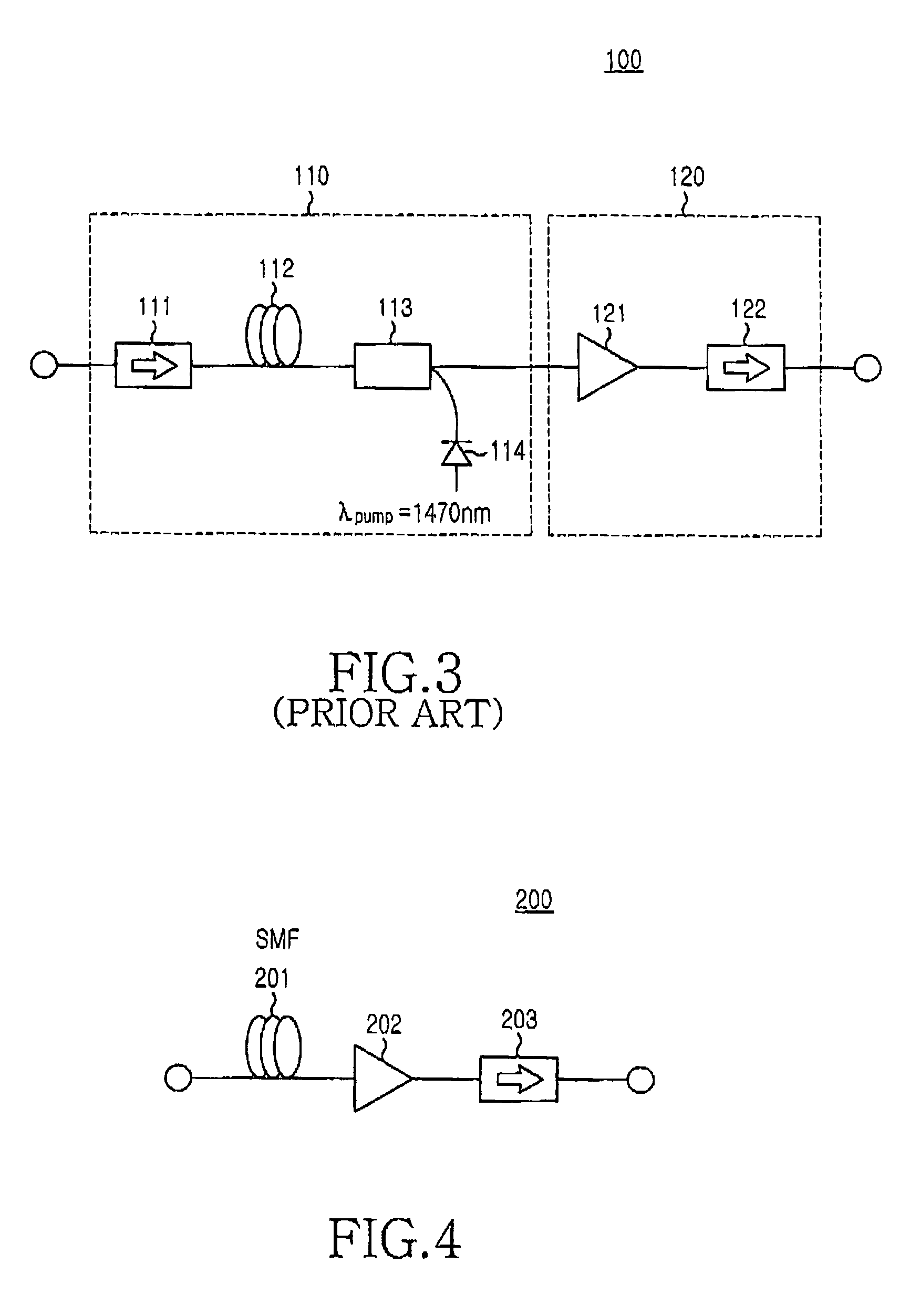
[0034]FIG. 4 is a construction view illustrating a gain-clamped semiconductor optical amplifier using the Raman amplification principle according to the present invention. The optical amplifier 200 comprises a single-mode fiber 201, a semiconductor optical amplifier 202, and an optical isolator 203.

[0035]The single-mode fiber 201, when being supplied with a pumping light, provides a gain on a longer wavelength side distanced about 100 nm from t...


PUM


Abstract

A gain-clamped semiconductor optical amplifier uses the Raman amplification principle. A Raman amplifier and a gain clamped semiconductor optical amplifier are integrated onto an optical amplifier module. The gain-clamped semiconductor optical amplifier includes: an optical fiber having Raman gain characteristics; and a gain-clamped semiconductor optical amplifier for providing a pumping light to the optical fiber by laser oscillation using a distributed Bragg reflector (DBR) lattice. The DBR has input and output terminals asymmetrical to each other, at least for amplifying a signal light Raman-amplified by the optical fiber.

Description

CLAIM OF PRIORITY[0001]This application claims priority to an application entitled “Gain-clamped semiconductor optical amplifier using Raman amplification principle,” filed in the Korean Intellectual Property Office on Jun. 11, 2003 and assigned Serial No. 2003-37481, the contents of which are hereby incorporated by reference.BACKGROUND OF THE INVENTION[0002]1. Field of the Invention[0003]The present invention relates to the use of optical amplifiers. More particularly, the present invention relates to a gain-clamped semiconductor optical amplifier using Raman amplification principle in which a Raman amplifier and a semiconductor optical amplifier are monolithic integrated with each other.[0004]2. Description of the Related Art[0005]In an optical communication system having transmitters and receivers, and fiber etc., the signal light emitted from a transmitter suffers from a transmission loss. As a result, the signal arriving at a receiver has less power than the signal originally t...

Claims


Application Information

Patent Timeline
IPC IPC(8): H01S3/00H01S3/06G02B6/26G02F1/015G02F1/39H01S3/063H01S3/094H01S3/0941H01S3/10H01S3/23H01S3/30H01S5/30H01S5/50
CPCH01S5/50H01S3/302H01S3/06754H01S3/2375H01S5/5072A63B57/40A63B2102/32G09F23/0066
Inventor LEE, JEONG-SEOKHWANG, SEONG-TAEK
Owner SAMSUNG ELECTRONICS CO LTD
Why Eureka
Try Eureka