Manufacturing method for microdisplay
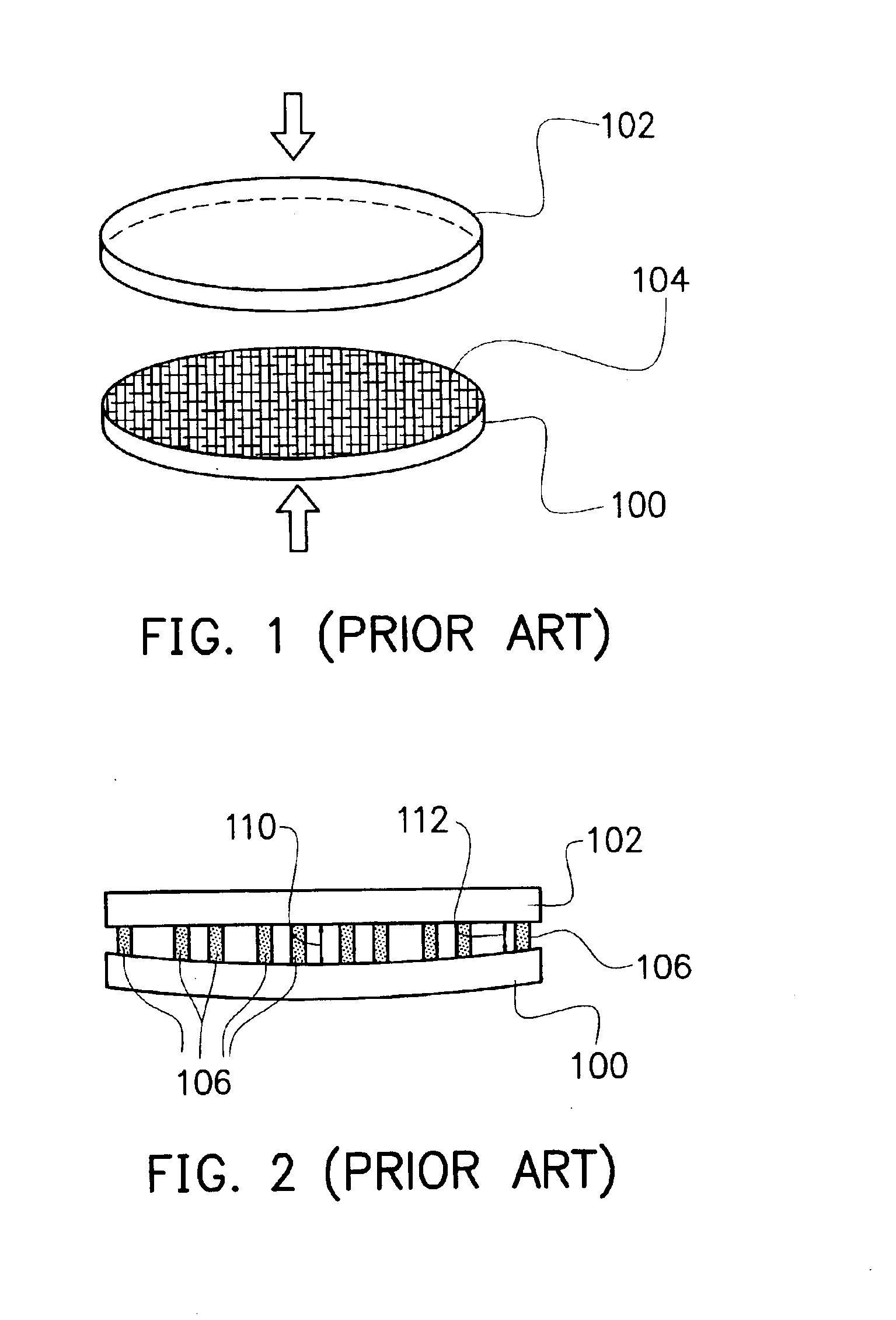
a manufacturing method and micro-display technology, applied in non-linear optics, instruments, optics, etc., can solve the problems of high quality and undeviating images, and achieve the effect of preventing the non-uniformity of gaps
- Summary
- Abstract
- Description
- Claims
- Application Information
AI Technical Summary
Benefits of technology
Problems solved by technology
Method used
Image
Examples
first embodiment
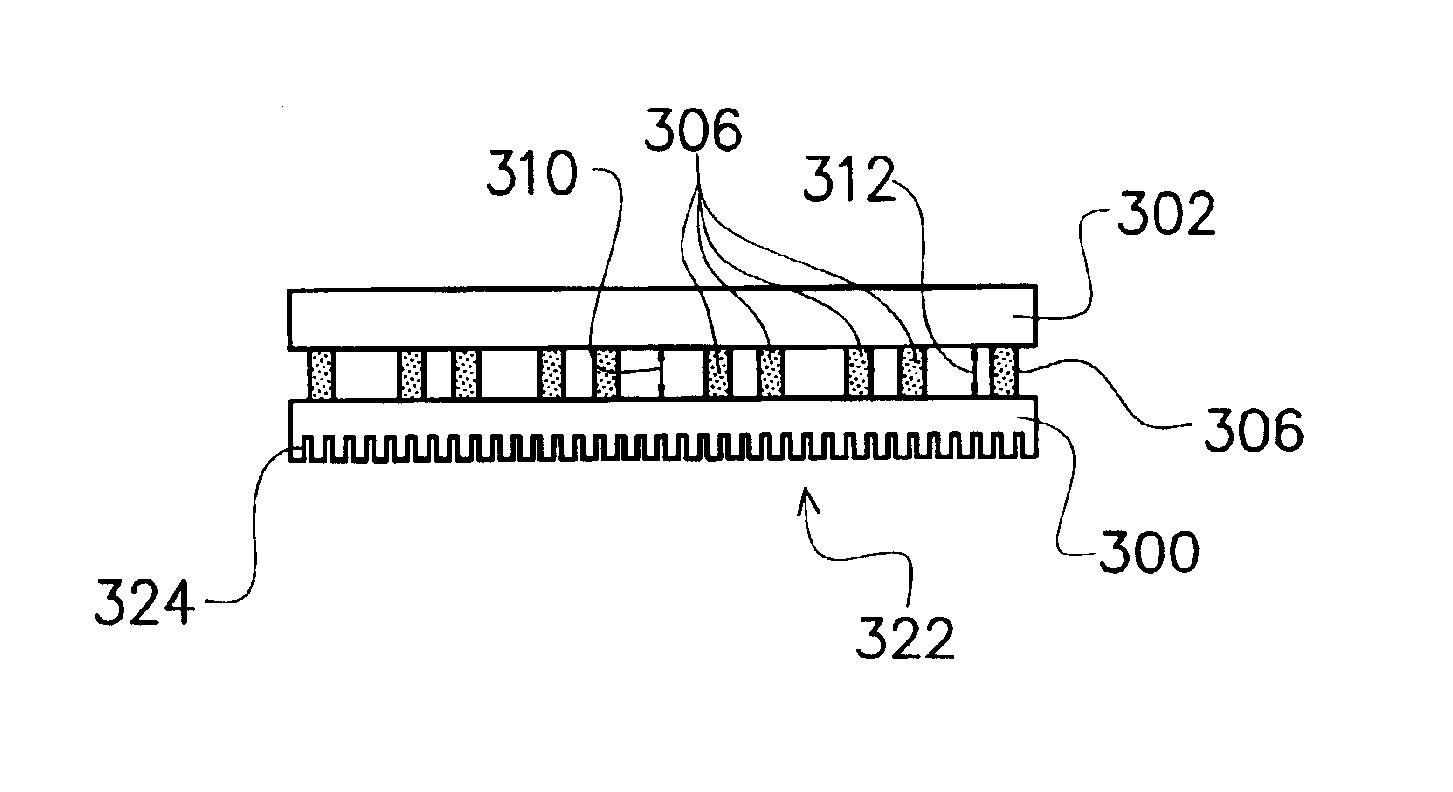
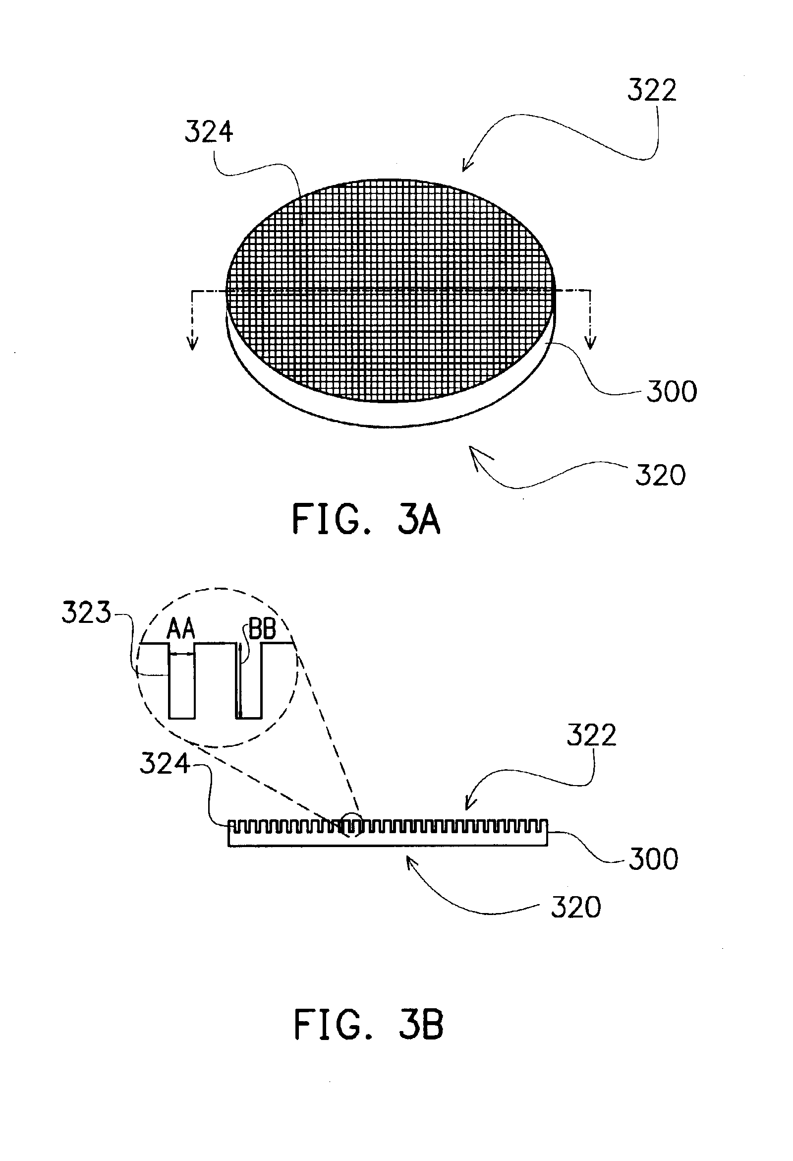
[0025]FIG. 3A is a three-dimensional view of a wafer substrate for a microdisplay after cutting according to the first preferred embodiment of the present invention, while FIG. 3B is a cross-sectional view of the wafer substrate of FIG. 3A. Referring to FIGS. 3A and 3B, a wafer substrate 300 is provided, while a plurality of pixel structures 304 (shown in FIG. 4) are formed on the front side 320 of the wafer substrate 300. For example, the wafer substrate 300 is a silicon wafer substrate. The backside 322 of the wafer substrate 300 is cut or sectioned in order to form trenches 323 with a pattern 324. The trenches are formed in a grid pattern or a checker pattern, or in other arranged patterns. As shown in an enlarged view (left side) for a portion of the wafer substrate in FIG. 3B, the trenches 323 of the grid pattern 324 have a width AA of about 50-150 microns and a depth BB of about 50-300 microns. For example, laser cutting is used to perform the cutting of the wafer substrate (t...
second embodiment
[0030]FIG. 7 is a flow chart showing the process steps for improving uniformity of the microdisplay according to the second preferred embodiment of the present invention. In step 700, a first substrate is provided with a plurality of pixel structures formed on the front side of the first substrate. In step 702, the backside of the first substrate is sectioned (cut) to form trenches with a pattern. The trenches are formed in a grid pattern or a checker pattern, or in other arranged patterns by, for example, laser cutting, while the trenches have a width of about 50-150 microns and a depth of about 50-300 microns.
[0031]In step 704, a sealant pattern is formed on the front side of the first substrate. In step 706, a second substrate is arranged above the front side of the first substrate, so that the first substrate is adhered to the second substrate.
[0032]In conclusion, the present invention has the following advantages:
[0033]Since the backside of the wafer substrate is sectioned to f...
PUM
| Property | Measurement | Unit |
|---|---|---|
| width | aaaaa | aaaaa |
| depth | aaaaa | aaaaa |
| transparent | aaaaa | aaaaa |
Abstract
Description
Claims
Application Information
 - R&D
- Intellectual Property
- Life Sciences
- Materials
- Tech Scout
- Unparalleled Data Quality
- Higher Quality Content
- 60% Fewer Hallucinations
Browse by: Latest US Patents, China's latest patents, Technical Efficacy Thesaurus, Application Domain, Technology Topic, Popular Technical Reports.
© 2025 PatSnap. All rights reserved.Legal|Privacy policy|Modern Slavery Act Transparency Statement|Sitemap|About US| Contact US: help@patsnap.com


