Solid-state device

a solid-state device and integrated circuit technology, applied in semiconductor devices, lasers, laser details, etc., can solve the problems of bare surface, inability to passivate perfectly, and expansion of peripheral surface, so as to improve device reliability and small geometries

Inactive Publication Date: 2005-12-27
LI CHOU H
View PDF22 Cites 4 Cited by
  • Summary
  • Abstract
  • Description
  • Claims
  • Application Information

AI Technical Summary

Benefits of technology

[0008]Therefore, to overcome the foregoing and other difficulties, the general object of this invention is to provide an improved, surf...

Problems solved by technology

These devices therefore often fail by surface or stress-related failure mechanisms.
However, such an expanded peripheral surface, being bare, is still not p...

Method used


Image

  • Solid-state device
  • Solid-state device
  • Solid-state device

Examples


Embodiment Construction

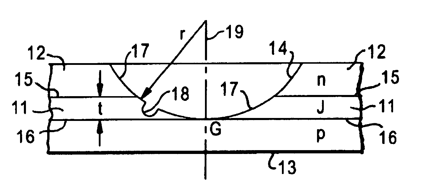
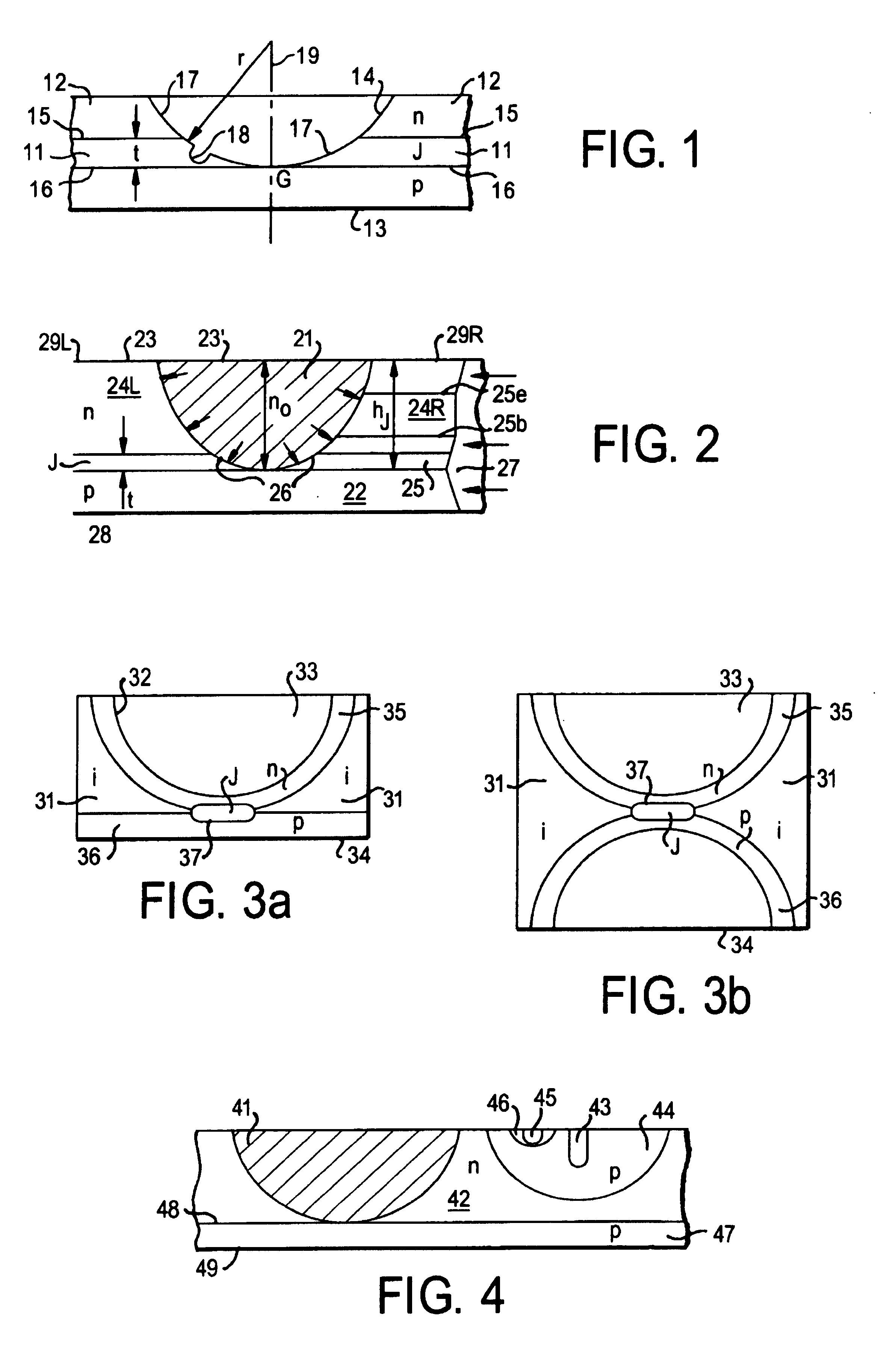
[0025]The PN junction devices of FIGS. 1-2 are sufficiently disclosed in all the referenced patents and patent applications. The '300 application, for example, specifically indicates that the pn junction devices of FIGS. 1-2 are sufficiently disclosed in my issued patent, U.S. Pat. No. 3,585,714. These are being redescribed (briefly) herein.

[0026]In the devices of FIGS. 1 and 2, the electrical signal current through the interfacial electronic barrier, such as a PN junction, is controlled by mobile carriers in the form of electrons and / or holes. The electronic barrier changes its electrically conductivity depending on the applied bias thereacross. For example, the PN junction is substantially electrically nonconductive under an applied reverse bias, but conductive under applied forward bias. This PN junction is a critical component in the functioning of many solid-state devices to be described herein.

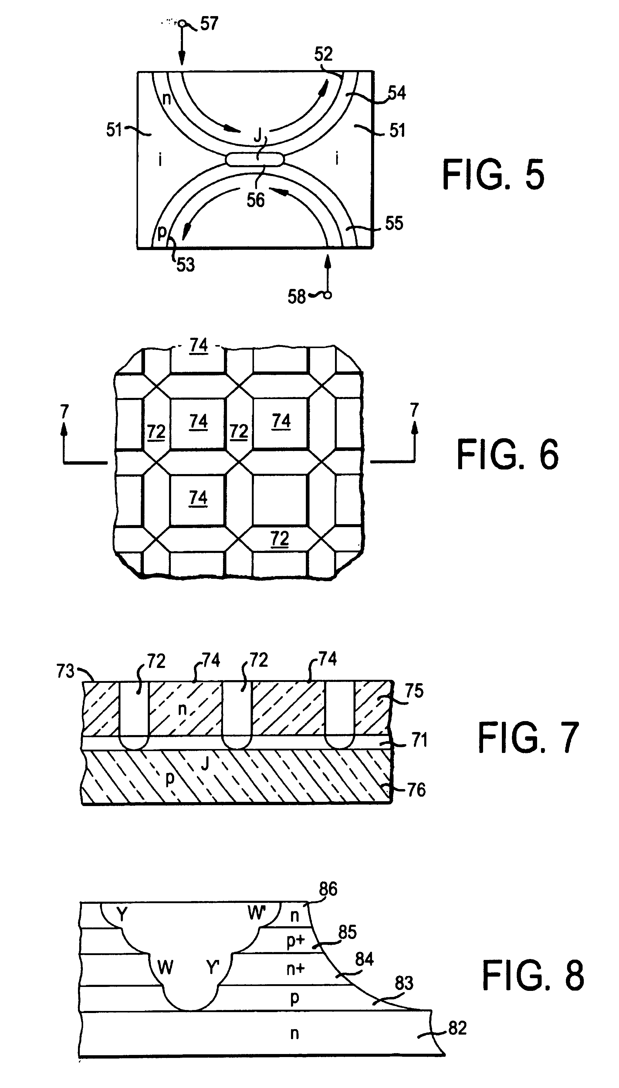
[0027]Other than PN junctions, metal-semiconductor or Schottky barriers, heterojunct...


PUM


Abstract

A method of making dielectrically isolated solid state device comprising state device (including integrated circuits) comprises providing a silicon wafer having a PN junction or other electronic rectifying barrier contained therein and thermally growing or ion-implanting selected ions to an oxide or nitride isolating groove in-situ to isolate it into a plurality of physically integral pockets for use as electrically separately operable components. The groove has a symmetrical, centrally rounded bottom which is located within a few microns below the PN junction or rectifying barrier. Through the unique oxide/nitride forming conditions and through curvature, symmetry, and proximity effects, novel passivation and isolation results obtain.

Description

CROSS-REFERENCE TO RELATED APPLICATIONS[0001]This is a continuation-in-part (CIP) of my applications Ser. Nos. 07 / 809,460 and 07 / 816,626, filed Dec. 31, 1991 and Dec. 9, 1991 both abandoned. Both of these applications are CIP's of my application Ser. No. 07 / 438,692, filed Nov. 17, 1989, now U.S. Pat. No. 5,082,793. The '692 application is a -continuation of application Ser. No. 05 / 386,102 filed on Aug. 6, 1973 and now U.S. Pat. No. 4,946,800and a continuation-in-part of application Ser. No. 838,758 and a continuation-in-part of application Ser. No. 05 / 838,758 filed on Oct. 3, 1977 and now U.S. Pat. No. 4,916,513. These '102 and '758 applications are CIPs of my application Ser. No. 05 / 154,300, filed Jun. 18, 1971, now abandoned. This '300 application is a CIP of my patent application Ser. No. 04 / 761,646, filed Sep. 23, 1968, now U.S. Pat. No. 3,585,714. The '646 application in turn is a CIP of my application Ser. No. 04 / 490,955, filed Sep. 28, 1965 and now U.S. Pat. No. 3,430,109. I ...

Claims


Application Information

Patent Timeline
IPC IPC(8): H01L21/762H01L29/00H01S5/024
CPCH01L21/76232H01S5/024H01S5/02423
Inventor LI, CHOU H.
Owner LI CHOU H
Why Eureka
Try Eureka