Isolation structures for imposing stress patterns

a technology of isolation structure and stress pattern, which is applied in the direction of semiconductor devices, electrical apparatus, transistors, etc., can solve the problems of not addressing the feasibility of any kind of device structure or method of fabrication, and the inability to improve both nfets and pfets simultaneously, so as to achieve enhanced performance and enhance performance

Inactive Publication Date: 2005-12-13
GLOBALFOUNDRIES US INC
View PDF3 Cites 138 Cited by
  • Summary
  • Abstract
  • Description
  • Claims
  • Application Information

AI Technical Summary

Benefits of technology

[0008]In this invention we show methods and structures by which we have applied in-plane biaxial (two-dimensional) tensile stress for the NFET while at the same time applying in-plane compressive longitudinal stress and a tensile transverse stress on the PFET device. The structures and methods of making each device individually is also unique. The primary advantage of these methods and structures is that they have provided two-fold device performance improvement relative to merely uniaxial stresses. Another advantage is the method for fabricating NFETs and PFETs simultaneously on a common substrate, wherein each device is designed to enhance performance using stress inducing isolation material. A secondary advantage is the structure and method of building an individual device with enhanced performance provided via stress inducing trench isolation structures.
[0009]It is an object of the present invention to provide device performance improvements for NFETs, PFETs, and for both NFETs and PFETs simultaneously. It is another object of the present invention to be readily integratible into present manufacturing processes cheaply for significant device performance improvements by adding a single mask step. It is another object of the present invention to be manufacturable in bulk silicon, silicon-on-insulator (“SOI”), and strained silicon structures.

Problems solved by technology

Prior known solutions and methods using mechanical stress for device performance enhancement could not improve both NFETs and PFETs simultaneously.
Moreover, prior solutions do not address the feasibility of any kind of device structures or methods of fabricating them.

Method used


Image

  • Isolation structures for imposing stress patterns
  • Isolation structures for imposing stress patterns
  • Isolation structures for imposing stress patterns

Examples


Embodiment Construction

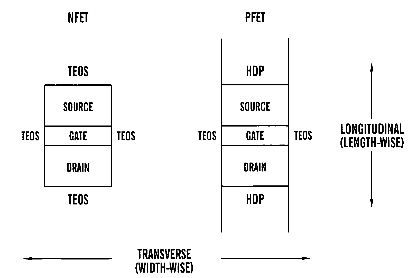
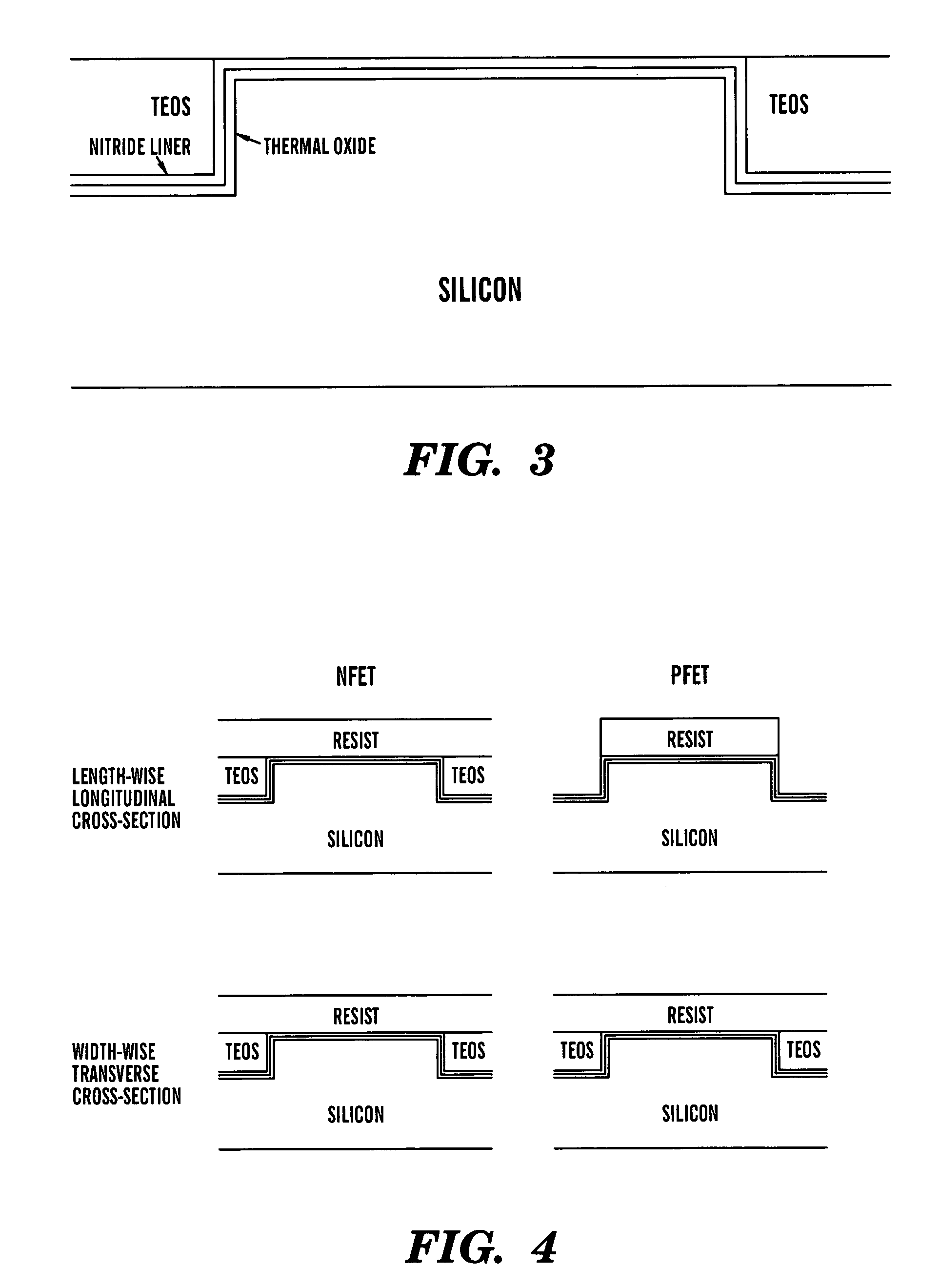
[0019]The present invention involves filling isolation regions, preferably shallow trench isolation (“STI”) with different intrinsically stress inducing materials to impart selected longitudinal and transverse stress components upon active device regions formed in a substrate. For example, using a stress inducing material that is intrinsically tensile causes a tensile state of stress in the substrate and an intrinsically compressive material causes compression in the substrate. In order to impart these different stresses in devices, we use deposited films that impose different intrinsic stresses. For example, TEOS (TETRAETHYLORTHOSILICATE) is known to be tensile because it undergoes densification under anneal and so it shrinks, thereby imposing upon an adjacent substrate a tensile stress. HDP (High density Plasma) oxide is known to be intrinsically compressive. The key here is to integrate two different intrinsically stress inducing structures adjacent the NFET and PFET structures o...


PUM


Abstract

A substrate under tension and / or compression improves performance of devices fabricated therein. Tension and / or compression can be imposed on a substrate through selection of appropriate STI fill material. The STI regions are formed in the substrate layer and impose forces on adjacent substrate areas. The substrate areas under compression or tension exhibit charge mobility characteristics different from those of a non-stressed substrate. By controllably varying these stresses within NFET and PFET devices formed on a substrate, improvements in IC performance are achieved.

Description

CROSS REFERENCE TO RELATED APPLICATIONS[0001]U.S. patent application Ser. No. 10 / 318,602, entitled “Stress Inducing Spacers” filed concurrently herewith is assigned to the same assignee hereof and contains subject matter related, in certain respect, to the subject matter of the present application. The above-identified patent application is incorporated herein by reference.BACKGROUND OF THE INVENTION[0002]1. Technical Field of the Invention[0003]This invention pertains to inventive methods of manufacturing a semiconductor device for improving device performance, and to the resulting unique high-performance device structure. In particular, this invention has improved charge mobility in FET devices by structurally imposing tensile and compression forces in a device substrate during device fabrication.[0004]Within the field of semiconductor device design, it is known that mechanical stresses within the device substrate can modulate device performance. Individual stress tensor component...

Claims


Application Information

Patent Timeline
Patent Type & Authority Patents(United States)
IPC IPC(8): H01L21/76H01L21/762H01L21/8238H01L29/80H01L31/109H01L31/112
CPCH01L21/76232H01L21/823807H01L29/7846H01L21/823878H01L29/785
Inventor CHIDAMBARRAO, DURESETIDOKUMACI, OMER H.DORIS, BRUCE B.MANDELMAN, JACK A.
Owner GLOBALFOUNDRIES US INC
Why Eureka
Try Eureka